Effect of Sn-incorporation on the Structural and Optical Properties of ZnO Thin Films Prepared by Sol-Gel Method
Hansraj Sharma* , Sunil Kumar, Jagavendra Yadav, Jagdish Prasad, and Mangej Singh
Department of Physics, University of Rajasthan, Jaipur, Rajasthan, India.
Corresponding Author E-mail: sharmahansraj313@gmail.com
DOI : http://dx.doi.org/10.13005/ojc/390614
Article Received on : 01 Sep 2023
Article Accepted on :
Article Published : 17 Nov 2023
Reviewed by: Dr. Vinoy Thomas
Second Review by: Dr. Navya Kumari
Final Approval by: Dr. Wasinton Simanjuntak
In this research, thin films of ZnO doped with Sn were prepared through the sol-gel method. The effects of Sn dopant on optical, morphological and structural studies were investigated. All of the films in this work showed favored orientation along the (002) plane, according to XRD analysis. It was observed by SEM analysis that the study Sn morphological and structural studies were investigated. From AFM pictures it is clear that as the doping concentration rises, the size of the grains on the surface of thin films decreases.The existence of Zn, O and Sn was verified by the EDAX analysis. The Ultraviolet-visible spectroscope was utilized to examine the optical characteristics. That band gap increased with the dopant material percent increased.
KEYWORDS:AFM; Doping; EDAX; Sol gel method; Spin coating; Structural; UV–Vis spectroscopy
Download this article as:| Copy the following to cite this article: Sharma H, Kumar S, Yadav J, Prasad J, Singh M. Effect of Sn-incorporation on the Structural and Optical Properties of ZnO Thin Films Prepared by Sol-Gel Method. Orient J Chem 2023;39(6). |
| Copy the following to cite this URL: Sharma H, Kumar S, Yadav J, Prasad J, Singh M. Effect of Sn-incorporation on the Structural and Optical Properties of ZnO Thin Films Prepared by Sol-Gel Method. Orient J Chem 2023;39(6). Available from: https://bit.ly/47V7j2z |
Introduction
One of the most significant and promising materials is ZnO, which is used in a variety many fields of study, as a solar cell 1 including gas sensors, laser diodes, thin film transistors, piezoelectric and optoelectronic devices2,3. There are several different ways to make ZnO thin films as RF/DC sputtering 4, Pulsed laser deposition 5, Spray pyrolysis [6] and the Sol-gel method 7. Among all of these processes, the sol-gel method is the most popular and draws a lot of research attention because its specific benefits, which include cheap cost, basic deposition equipment, ease of altering composition and dopant and the ability to fabricate large area films8. It has a stable hexagonal wurtzite structure and direct wide band gap 3.4eV n-type semiconductor with a high binding energy (60 meV) is zinc oxide (ZnO), which has an ambient temperature to exhibits good chemical and thermal stability 9. The tetravalent metal dopants, such as silicon Indium 10, Germanium (Ge), Aluminum 11, Cobalt 12, Tin 13, Titanium (Ti) 14 and others, are added to ZnO films to increase their conductivity. Sn is a beneficial material among these tetravalent metal dopants because it has good optical transmittance 15.Recently, there has been extensive research into the hydrogen gas sensors properties of oxide (SMO) thin films. Hydrogen sensors utilizing metal oxides like SnO2, TiO2, NiO, and ZnO demonstrate remarkable sensitivity, enabling rapid detection of trace amounts of hydrogen gas in the air16,17. A hydrogen sensor serves as a primary mechanism for early detection of hydrogen leakage and continuous monitoring of hydrogen status18. One of the most successful methods for increasing ZnO’s photo catalytic performance is doping with metal ions 19,20. Sn Doping can increase the photo catalytic activity of ZnO by modifying its surface morphology, localized states and band gap 21.
Therefore, in this study Undoped, 2% and 4% Tin doped ZnO thin films were used by the spin coating method and their physical characteristics have been investigated in order to comprehend the impact of tin doping level, also study the structural properties and changes in optical properties, mainly the variation in the band gap. The Study of Sn doping interpretation, the surface morphology and roughness were also examined.
Experimental procedure
Chemicals and Materials
Zinc acetate dihydrate, Tin chloride (SnCl₄), Solvent, Substrate as a glass slide, Annealing furnace, Magnetic stirrer and hot plate, Glass container, and characterization equipment.
Preparation of Precursor Solution
The creation of an aqueous Tin doped Zinc Oxide(SZO), 2M zinc acetate dehydrates and Tin Acetate {Sn(CH3COO)4} were dissolved in the solution 2-Methoxy Ethanol and HCL. Subsequently, Mono Ethanolamine (MEA) was incrementally into the solution as a stabilizing agent, with a Zinc Acetate dihydrate. While adding the proper quantity of tin chloride to a clear solution during a 4-hour period at 60°C; the zinc precursor solution should be continually stirred. The [Sn4+]/ [Zn2+] nominal ratio solution was Undoped, 2% and 4% Sn-doped for 24 hours kept at room temperature. Then the solution was put onto the pre-cleared glass substrate, which was then spun for 35 seconds at room temperature at 2800 rpm. The solvent was then removed from the films by drying them over a hot plate for 8 minutes at 120°C following the procedure of spin coating deposition until the necessary film thickness for processing had been obtained, the process of drying was repeated. The generated multi layered ZnO films were annealed in a muffle furnace for about 2 hours at a temperature of 550℃.
 |
Figure 1: Experimental a research method of prepared Undoped, 2% and 4% Tin doped ZnO thin Film. |
Result and Discussion
ZnO Thin Films structural characterization
Fig.2 depicts the evolution of the XRD structures for Undoped, 2% and 4% Tin-doped ZnO thin films.Cu Kα, radiation with λ=1.5425 Aº inside the range from (20º to 80º) was used to create the XRD pattern. Compare peaks with JCPDS card no. 04-008-8198. All of the observed peaks were found to be inside the structure of hexagonal wurtzite of ZnO. Undoped ZnO thin film is polycrystalline according to XRD patterns and the peaks with the highest intensities have been identified at 2θ=31.64, 34.30, 36.13, 47.43, 56.49, 62.73 and 67.83 at planes (1 1 1), (0 0 2), (1 0 1), (1 0 2), (1 1 0), (1 0 3), (1 1 2) accordingly, as indicated in Fig. 2. Furthermore, Sn doped ZnO thin films have showed the several Sn element related peaks that can be seen in undoped ZnO and demonstrate that all samples have the preferred direction in the (0 0 2) as seen in Fig-2. This suggested that the Sn doping and ZnO lattice are closely linked. The appearance of new peaks at shorter distances is attributed to the formation of Zn-Sn (OH), resulting from an ion exchange process between HCL and chloride acid. 22.
Scherrer formula was used for the average crystalline size of the samples.
By Scherrer’s formula
D = 0.9 λ / β cos (θ)……… (1)
Here:
λ→ wavelength of X-ray diffraction(1.5425 Å),
θ → Bragg diffraction angle, and β→ Full width half maximum(FWHM).
 |
Figure 2: XRD pattern for Undoped, 2% and 4% Sn-doped Zinc Oxide thin films. |
The XRD of Sn doped Zinc Oxide shown in Fig. 2 indicates a strong orientation of Sn peak (002) in the XRD pattern and other peaks (100),(101),(102),(110),(103) and (112) belongs to Zinc Oxide. These peaks well match with Compare peaks with JCPDS card no. 04-008-8198.The measured crystalline size changed as the Sn doping (0–4%) was varied shown in Table 1. It shown that Crystalline Size reduces significantly after Sn doping. The findings align with the Raman spectroscopy measurements depicted in the fig-3 and the Raman spectrum was acquired using a Raman Microscope with the literature 23.
 |
Figure 3: Raman spectra graph for Undoped, 2% and 4% Sn doped ZnO thin films. |
Table 1: The XRD data of Undoped, Sn-doped 2% and 4% ZnO thin films.
|
Sample name |
2θ |
FWHM |
D(nm) |
d(Aº) |
δ*10-4 (nm)-2 |
|
Undoped ZnO |
34.44 |
0.81 |
1.78 |
2.602 |
3156 |
|
ZnO with Sn 2% |
34.34 |
0.99 |
1.46 |
2.609 |
4691 |
|
ZnO with Sn 4% |
34.37 |
1.1 |
1.31 |
2.607 |
7817 |
Increased doping concentration results in a rise in the dislocation density (δ). It is obvious that crystalline is declining because of the decline in crystalline size and the corresponding enhancement in other metrics (Dislocation density) with rising Sn dopant concentration 24.
Surface Morphology for Sn-doped ZnO thin films
SEM Analysis
Fig.4 displays the surface morphology of Tin-doped ZnO thin films which were created at various dopant Undoped, 2% and 4% concentrations. According to the Sn concentration, each film has a distinct morphology as shown in the SEM images. All films had uniform and constant microstructures across the surface.
 |
Figure 4: SEM pictures for (A) Undoped, (B) Sn 2% and (C) Sn 4% Zinc Oxide thin films. |
Additionally, when doping concentration grew, that change the density of the microstructure. We hypothesized that raising the doping concentration reduced the size of grain of Sn doping thin film and that tiny grain does not produce any pores. According to the author 25 the observed spherical grain morphology which well match with our SEM photograph. The Crystalline size of the (002) peak at different Sn doping concentrations Undoped, 2% and 4% are 100.47nm, 95.76nm and 84.66nm so when doping concentration increased grain size decreased.
AFM images
Fig.5 shows AFM pictures of the surface morphology that were produced at different solution volumes Undoped, 2% and 4% Tin doped.Fig.5 also displayed the surface topographies of the spin-coated Zinc Oxide thin films in 2D and 3D. In this work the surface topography of the thin films sample may be investigate using the Atomic Force Microscope (AFM), which is a popular method.
 |
Figure 5: The AFM pictures of (A) Undoped,(B)Sn2% and (C)Sn4%- doped ZnO thin films |
The SEM data carried out by us; suggest that raising the doping concentration caused a decrease the ZnO structures in a crystalline form and their surface roughness. The mean roughness of ZnO films having different Sn doping concentration Undoped, 2% and 4% are 0.2059 nm, 0.2030nm and 0.2023nm respectively. According to AFM images, the grain size and clusters on the surface of films improved, when the doping concentration was raised the roughness decreased. Correspond to those reported in the literature 26.
EDAX Spectrum
Sn doped ZnO films were elementally analyzed by Energy Dispersive Spectroscopy (EDS),is shown in Fig.6 made at temperature 550°C. It revealed that the elements zinc and oxygen are nearly stoichiometrically present (56:41) %.
 |
Figure 6: Chemical composition of (A) Undoped, (B) Sn2% and (C) Sn4% doped ZnO films. |
The EDAX analysis of the Tin-doped ZnO thin films indicated the presence of Tin, Zinc and Oxygen.Sn-doped EDAX spectra Supplementary peaks relating to Sn, zinc and oxygen were observed in ZnO thin films. This research demonstrated Sn ion assimilation into the ZnO lattice. According to our conclusions, the Sn weight percentage was discovered to rise with an increase in Sn-dopant concentration.The glass substrate gave rise to the Si peaks in the EDAX spectrum.
ZnO Thin Films Optical properties
This part specified all the foundations of mathematics for optical constants using UV-Vis measurements. The first parameter that is calculated by the method that follows is the absorption coefficient 27:
α = 2.303 (A/t) ….… (2)
There α →Absorption coefficient, t → thickness and A → absorbance.
The Famous Tauc formula is applied to calculate the energy band gap value 28
(αhν)² =A (hν – Eg)n……. (3)
where n is the index density of the states with A, h and v as the absorption Constant, Plank constant and Frequency respectively of incoming light and Eg is the energy gap.
 |
Figure 7: Transmittance spectra of Undoped, Sn 2% and Sn4% doped ZnO thin films. |
Fig.7 displays the transmittance spectra (T) for Undoped, Sn2% and Sn4% doped ZnO thin films at different concentrations, all measured in the (280-600 nm) wavelength range.
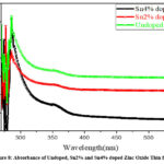 |
Figure 8: Absorbance of Undoped, Sn2% and Sn4% doped Zinc Oxide Thin films. |
According to Fig.8, all of the samples absorbance peaks at short wavelengths around the visible spectrum’s boundary of primary absorption. After that, it decreases for doped films with increasing wavelength. For doped ZnO films, the absorption spectra decrease with increasing wavelength. Using the values of the absorption coefficients the energy gap was calculated. Fig.9 depicts the relation between (αhv) 2 and hv, where hv is the energy of the incident photon and α represents the optical absorption coefficient.
 |
Figure 9: Energy band gap of Undoped,Sn2% and Sn4% doped ZnO thin films. |
Table 2: Energy band gap value of Undoped, 2% and 4% doped ZnO Thin films.
|
Sample |
Energy band gap(eV) |
|
Undoped ZnO |
3.59 (eV) |
|
ZnO with Sn 2% |
3.67 (eV) |
|
ZnO with Sn 4% |
3.77 (eV) |
The band gap for all samples determined using Eq. (3) was 3.59eV for undoped ZnO, 3.67eV for Sn 2% and 3.77eV for Sn 4% doped ZnO. The doped ZnO thin films observed band gap increased as mentioned in Table 2 and seen in Fig.9 and similar behavior was observed that band gap increased with decreased XRD intensity by Jagavendra et al 29. The efficiency of creating nano-scale devices using these materials is boosted as a result of the band gap increase.
Conclusions
In this study, the low-cost and straight forward sol-gel method has been used to synthesis Undoped, Sn 2% and Sn 4% doped ZnO thin films in a variety of volume concentrations. Investigated were the effects of Sn concentrations on both the optical and structural characteristics of ZnO thin films. XRD studies discover the hexagonal structure of prepared Sn-doped and Undoped ZnO thin films. This outcome was in line with that of the SEM images, rice-like morphology was appropriate to all spray-provided ZnO thin films. According to AFM pictures, the grain size and clusters on the surface of ZnO thin films decrease the concentrations of dopants percentage increase. The band gap for all samples determined was 3.59eV for undoped ZnO, 3.67eV for Sn 2% and 3.77eV for Sn 4% doped ZnO thin films marginally increased. We analyze that when the crystallinity decreased band gap value increased.
Acknowledgment
Mr. Hansraj Sharma thanks the MNIT MRC and Manipal University, Jaipur for providing characterization resources for this research. Many thanks to USIC (UOR) and the Physics Department at University of Rajasthan in Jaipur for providing the test and characterization facilities.
Conflict of interest
On behalf of all the authors, the corresponding author affirms that there are no conflicts of interest.
Funding Sources
There is no funding sources.
References
- Fenglin, X.; Kaibo, M.; Xuecheng, B.; Yun, J.Characterization of Ag-doped ZnO thin film synthesized by sol-gel method and its using in thin film solar cells.Optik, 2013,124, 4876-4879.
CrossRef - Jiabao, C.; Dejun, W.;Tengfeng, X.; Yanhong, L.Study on photoelectric gas sensing property and photogenerated carrier behavior of Ag-ZnO at the room temperature. Sensors and Actuators B 186,2023, 165-171.
CrossRef - Bhattacharyya, P.; Basu, P.K.;Saha, H.; Basu S.Fast response methane sensor using nanocrystalline ZnO thin films derived by sol-gel method. Sensor and ActuatorB 124,2007, 62-67.
CrossRef - Duan, Li.; Xiaochen, Yu.; Lei, Ni.; Wang. Z.ZnO:Ag film growth on Si substrate with ZnO buffer layer by rf sputtering. Applied Surface Science 2011,257, 3463-3467.
CrossRef - Deuk, H.L.; Ki, H.P.; Sangsig, K.; Sang. Y.L.Effect of Ag doping on the performance of ZnO thin film transistor. The solid Films 2011,520, 1160-1164.
CrossRef - Tarwal, N.L.; Patil.P.S.Enhanced photoelectrochemical performance of Ag–ZnO thin films synthesized by spray pyrolysis technique. Electrochimica Acta 2011,56, 6510-6516.
CrossRef - Foo, K.L.; Kashif, M.; Hashim, U.; Liu, W.W.Effect of different solvents on the structural and optical properties of zinc oxide thin films for optoelectronic applications. Ceramics International 2014,140 753-761.
CrossRef - Tripathi, A.; Misra, K. P.; Shukla, R. UV enhancement in polycrystalline Ag-doped ZnO films deposited by the sol–gel method. Journal of Luminescence, 149, 361-368(2014).
CrossRef - Karthick, A.; Umadevi G.; andPradhabhan, D. Structural, Optical and Antibacterial Activity Studies of Sn Doped Zno Thin Films Prepared by Chemical Spray Pyrolysis Technique.Int. J.Res. Anal. Rev.2018, vol. 5, issue 4.
- Kumar, P.; Dev, S.;Kumar,A.; Thakur,R.; Dhar R. Impact of indium doping on the anti-biofilm activity of ZnO thin films against Escherichia coli and Staphylococcus aureus. Superlattices and Microstructures,2021,150.
CrossRef - Van Toan, N.; Tuoi, T. T.; Inomata, N.; Toda, M.; Ono, T. Aluminum doped zinc oxide deposited by atomic layer deposition and its applications to micro/nano devices. Scientific Reports, 11(1), 1-12 (2021).
CrossRef - Kumar, D.; Singh, M. K.; Mehata, M. S. Exploration of grown cobalt-doped zinc oxide nanoparticles and photodegradation of industrial dye. Materials Research Bulletin, 150, 111-795 (2022).
CrossRef - Aydin,H.; El-Nasser,H.M.; Aydin,C.; Al-Ghamdi,A.; and Yakuphanoglu,F. Synthesis and characterization of nanostructured undoped and Sn-doped ZnO thin films via sol-gel approach.Appl. Surf. Sci., vol. 350, pp.2015, 109–114.
CrossRef - Sarathi,R.;Sheeba,N.L.;Selva,E.;Essaki, andSundar,S.M. Titanium doped Zinc Oxide nanoparticles: A study of structural and optical properties for photocatalytic applications. Materials Today: Proceedings,2022,64, 1859–1863.
CrossRef - Liu,X.;Wu,X.;Cao,H.; Chang, R.P.H. Growth mechanism and properties of ZnO nanorods synthesized by plasma-enhanced chemical vapor deposition. J. Appl. Phys. 95 ,2004,3141-3147.
CrossRef - Chou,P.C.; Chen,H.I.; Liu,I.P.; Chen,C.C.; Liou,J.K.; Hsu,K.S.; Li,W.C. Hydrogen sensing performance of a nickel oxide (NiO) thin film-based device. Int. J. Hydrog. Energy 2015, 40, 729–734.
CrossRef - Zhang, H.; Jia, H.; Ni, Z.; Li, M.; Chen, Y.; Xu, P.; Li, X. 1ppm-detectable hydrogen gas sensors by using highly sensitive P+/N+ single-crystalline silicon thermopiles. Microsystems & Nanoengineering, 9(1), 1-11 (2023).
CrossRef - Lee,J.S.;An,J.W.;Bae,S.; and Lee,S.K. Review of Hydrogen Gas Sensors for Future Hydrogen Mobility Infrastructure. Applied Science and Convergence Technology,2022,31(4), 79–84.
CrossRef - Dodd,A.C.; McKinley,A.J.; Saunders,M. Effect of Particle Size on the Photocatalytic Activity of Nanoparticulate Zinc Oxide. J Nanopart Res 8, 43–51 (2006).
CrossRef - Becker,J.;Raghupathi,K.R.; Pierre,J.S. Tuning of the crystallite and particle sizes of ZnO nanocrystalline materials in solvothermal synthesis and their photocatalytic activity for dye degradation. J Phys Chem C. 2011;115:13844–13850.
CrossRef - Salvi, S.; Lokhande, P.B.; Mujawar. H.A.Degradation of recalcitrant phenol pollutant and antibacterial study by Ni, Sr doped ZnO. Inorg Nano-Meta Chem. 2020,50:114–123.
CrossRef - Bhatia,D.;Sharma,H.;Meena,R.S. and Palkar.V.R.A novel ZnO piezoelectricmicrocantilever energy scavenger: Fabrication and characterization, Sens. Bio-Sensing Res., 2016,vol. 9, pp. 45–52.
CrossRef - Zuo,Z.; Zhu,K.; Gu,C.; Wen,Y.Cui,G. Qu, J. Transparent, flexible surface enhanced Raman scattering substrates based on Ag-coated structured PET (polyethylene terephthalate) for in-situ detection. Applied Surface Science.2016, 379, 66-72.
CrossRef - Alvarado J.A.; Maldonado, A.; Juarez, H.; Pacio, M. Synthesis of Colloidal ZnO Nanoparticles and Deposit of Thin Films by Spin Coating Technique, Journal of Nanomaterials, vol. 2013, 903-191 (2013).
CrossRef - Reddy,J.R.; Mani,G.K.; Shankar,P.; RayappanJ.B.B.Substrate temperature effects on room temperature sensing properties of nanostructured ZnO thin films. Journal of Nanoscience and Nanotechnology.2016,16(1), 489–496.
CrossRef - Ajili,M.; Castagné,M.; Turki, N.K. Study on the doping effect of Sn-doped ZnO thin films. Superlattices and Microstructures.2013,53(1), 213–222.
CrossRef - Sharimla,B; Singha, M. K.; Dwivedi, P. Impact of annealing on structural and optical properties of ZnO thin films. Microelectronics Journal, 135, 105-759 (2023).
CrossRef - Muchuweni, E.; Sathiaraj, T.; Nyakotyo, H. Synthesis and characterization of zinc oxide thin films for optoelectronic applications. Heliyon, 3(4), e00285. (2017).
CrossRef - Yadav,J.;Prasad,J.; Sharma,H.;Kumar,S.; Singh, M. Effect of Zn and Sn incorporation on the crystallinity of spin-coated CuInSe2 thin films. Journal of Materials Science: Materials in Electronics.(2022). 33. 1-10.
CrossRef

This work is licensed under a Creative Commons Attribution 4.0 International License.
About The Author
![]()
A New Edition of Web of Science
Journal Impact Factor
2022: 0.5
Five Year: 0.8
Journal is Indexed in

Cabells Whitelist
![]()


