Cu2ZnSnS4 Thin Film Solar Cell Construction Using Chemical Technique
Kishore Kumar Y B1* , Suresh Babu G2, Swapna Smitha A S2, Surya Sekhar Reddy M3 and Kiran Y B4
1Solar Energy Laboratory, Mohan Babu University (Erstwhile Sree Vidyanikethan Engineering College), Tirupati, 517102, India.
2Department of Physics, Government Degree College, Puttur, 517583, India.
3Department of Physics, Government Degree College for Women, Madanapalle,517325, India.
4Applied Chemistry Research Lab, Mohan Babu University, Tirupati, 517102, India.
Corresponding Author E-mail: ybkksvu@gmail.com
DOI : http://dx.doi.org/10.13005/ojc/390622
Article Received on : 27 Oct 2023
Article Accepted on : 06 Dec 2023
Article Published : 19 Dec 2023
Reviewed by: Dr. Randhir Rai
Second Review by: Dr. Pragya Sinha
Final Approval by: Dr. Tawkir Sheikh
Cu2ZnSnS4 (CZTS) presents itself as a potential quaternary semiconductor absorber layer in the field of thin film heterojunction solar cells. The conventional spray pyrolysis method has been used in the present investigation. X-ray diffraction results confirm the structure of the deposited films as kesterite. The lattice parameters are determined to be a = 0.5436 nm and c = 1.0856 nm. The material exhibits an energy gap of 1.5 eV and an optical absorption coefficient exceeding 104 /cm. CZTS films exhibit a p-type nature. The deposited films are kept on the hot surface for some time after the chemical spray pyrolysis is finished, which contributes to improved crystallinity. Using chemical synthesis techniques, a Cu2ZnSnS4 thin film solar cell is constructed. These solar cells exhibited an efficiency of 0.5%. Ongoing efforts are directed towards achieving reasonable efficiency levels.
KEYWORDS:Cu2ZnSnS4; Chemical spray pyrolysis technique; Heterojunction solar cell; Solar cell absorber material; Thin films
Download this article as:| Copy the following to cite this article: Kumar Y. B. K, Babu G. S, Smitha A. S, Reddy M. S. S, Kiran Y. B. Cu2ZnSnS4 Thin Film Solar Cell Construction Using Chemical Technique.Orient J Chem 2023;39(6). |
| Copy the following to cite this URL: Kumar Y. B. K, Babu G. S, Smitha A. S, Reddy M. S. S, Kiran Y. B. Cu2ZnSnS4 Thin Film Solar Cell Construction Using Chemical Technique.Orient J Chem 2023;39(6). Available from: https://bit.ly/3RREL4A |
Introduction
Electricity is indispensable in modern life and plays a crucial role in the economies of all nations. Various sectors such as industry, agriculture, transportation, and entertainment heavily rely on electricity. Energy sources are categorized into two main groups i.e., renewable and non-renewable sources. The former includes solar energy, wind energy, and bioenergy, while the latter comprises coal, oil, nuclear power, and other fossil fuels. Due to the extensive use of non-renewable sources, it is anticipated that these resources will be drained out within the next 30 years1. As a result, renewable energy sources have gained popularity in the 21st century. Solar energy, in particular, is an attractive option, especially for tropical countries like India. It has the potential to generate 4000 trillion kWh of energy in a day2. If some of this solar energy has been converted by solar cells into electric energy, the scarcity of energy sources might be minimized3.
The high cost of silicon-based solar cells has led researchers to focus on thin film solar cells. Solar cells grown by utilizing Cu(In,Ga)Se2 and CdTe as absorber layers have shown maximum conversion efficiencies of 26.4% and 22.1%, respectively4. However, these absorbers contain harmful elements like cadmium and selenium, as well as costly materials such as indium and gallium, limiting their applications. In light of these limitations, Cu2ZnSnS4 thin film absorbers have emerged as an alternative optoelectronic material for Cu(In,Ga)Se2 and CdTe solar cells. Cu2ZnSnS4 belongs to I2-II-IV-VI4 and is a promising quaternary semiconductor with optical and electrical properties similar to Cu(In,Ga)Se2 thin films5. Furthermore, Cu2ZnSnS4 films exhibit p-type electrical conductivity, kesterite structure, a direct energy band gap between 1.45-1.60 eV, and a high optical absorption coefficient. Especially, all the components of this semiconductor are abundant, cost-effective, and environmentally friendly6.
Various physical, as well as chemical techniques, have been employed to grow Cu2ZnSnS4 thin films. These techniques include pulsed laser deposition7, co-sputtering8, hybrid chemical approach9, chemical bath deposition10, two-stage process11, spin coating12, sol-gel methods13, and spray pyrolytic techniques14,15. The current study utilizes the spray pyrolytic method to deposit these thin films, which is an efficient, simple, and non-vacuum approach. This method allows for reproducible film production, and particle size control can be achieved by adjusting process parameters like solution flow rate, deposition time, substrate temperature, carrier gas, and vapor pressure of the gas, etc.,16-18.
Generally, in the spray deposition technique, the films are removed from the hot substrate after completing the chemical spray pyrolysis. After pyrolysis, the deposited films were kept remains on the hot substrate for a sufficient time which influenced the solidification and adherence of the films, this effect was addressed in this study. The structural, morphology, optical, elemental, and electrical analyses of the chemically synthesized films were investigated. Finally, a typical CZTS thin film heterojunction solar cell is fabricated.
Materials and Methods
Cu2ZnSnS4 films were deposited using a precursor solution that included salts of cupric chloride (9×10⁻³ M), zinc acetate (5×10⁻³M), stannic chloride (5×10⁻³M), and thiourea (5×10⁻² M)19. The excess thiourea in the precursor solution was deliberately higher than required to compensate for the sulfur loss during the experimentation. These Cu2ZnSnS4 films were grown on glass substrates that had been thoroughly cleaned by using chemically and ultrasonically. The well-cleaned glass substrates were then placed on a heated steel plate. Temperature measurements were conducted using a K-type thermocouple. The films were successfully grown at an optimized substrate temperature (370 °C), solution pH (3.2), and solution flow rate (10 ml/min)20-22. The spray nozzle was arranged at a height of 30 cm from the glass substrates23. The electric heater and the imported spray nozzle (Make: Spraying Systems, USA) were arranged inside the fume cupboard. An exhaust fan was incorporated into the fume cupboard to dissipate any generated gas fumes. The details of this experiment setup were discussed in our previous article3,19.
An effort was made to enhance the crystallinity of the Cu2ZnSnS4 films. To accomplish this, after the chemical spray pyrolysis, the deposited Cu2ZnSnS4 films remained on a hot plate at a constant temperature of 370 °C for 15 minutes. Finally, to facilitate the growth of CdS thin films as a buffer layer, chemical bath deposition was employed on the Cu2ZnSnS4 films. Detailed information about the experimental procedures can be found in our previously published article24.
The X-ray diffraction spectra of these films were recorded with a Bruker X-ray diffractometer using Cu-Kα radiation. The Raman spectrum of these films was recorded using an Ar+ laser source with a wavelength of 5143 Å under backscattered mode. X-ray photoemission spectra were recorded with X-ray photoelectron spectroscopy (XPS) spectra with Al Kα radiation. A Jeol scanning electron microscope (SEM) was utilized to examine the films’ surface morphology. Furthermore, the chemical composition of these films was analyzed with a traditional energy dispersive analysis X-ray spectrometer (EDAX). Using a Perkin Elmer double-beam spectrometer, the films’ spectral transmittance and reflectance were recorded. Finally, the conductive type of deposited films was identified through the hot probe method.
Results and Discussions
The Cu2ZnSnS4 films were extremely adherent to the glass substrates and homogeneous.
EDAX Analysis
The elemental analysis of the Cu2ZnSnS4 thin films is tabulated in Table 1. The first row gives information on the elemental analysis of the spray-deposited Cu2ZnSnS4 thin films which were immediately extracted from the hot plate after deposition. The later row confirms the composition of Cu2ZnSnS4 films which were left on the hot plate for 15 minutes after the spray pyrolysis and then were extracted. The composition analysis confirms the deposited thin films were slightly zinc-rich and had a slight copper deficiency. It’s worth noting that for optimal Cu2ZnSnS4 solar cell performance, conditions favoring a copper deficiency and zinc-rich are preferred6,25. Furthermore, when the samples were copper-deficient, this led to reduced binary impurities. The sulfur composition experienced a slight decrease when the films were left on the hot plate for 15 minutes after deposition and subsequent extraction. The volatility of sulfur may be the reason for the reduction in the films.
Table 1: Compositional analysis of Cu2ZnSnS4 thin films
|
Type of film |
Elemental composition (at. %) |
Composition ratio |
|||||
|
Cu % |
Zn % |
Sn % |
S % |
Cu/(Zn+Sn) |
Zn/Sn |
S/Metal |
|
|
Immediately extracted |
25.9 |
14.2 |
13.4 |
46.5 |
0.94 |
1.06 |
0.87 |
|
Extracted after 15 min. of deposition |
26.5 |
14.5 |
13.3 |
45.7 |
0.95 |
1.09 |
0.84 |
Structural Studies
The XRD pattern of Cu2ZnSnS4 films, extracted immediately from the hot substrate after pyrolysis was shown in Fig. 1(a), and films that were left on the hot plate for 15 minutes after the spray pyrolysis and then were extracted was illustrated in Fig. 1(b). Both films exhibited a preferred orientation along the (112) crystal plane. The distinct peaks corresponding to (112), (220)/(204), and (312)/(116) confirm the kesterite structure of the Cu2ZnSnS4 films, as supported by previous research6,27, and these peaks were also consistent with JCPDS card No. 26-0575. Notably, the XRD spectra revealed a significant increase in peak intensity when the deposited films were allowed to be kept on the hot substrate for 15 minutes after pyrolysis. Intensity ratio of I(112)/I(204) showed improvement in the deposited films that had undergone this additional heat treatment. A comparison between Fig. 1(a) and 1(b) also revealed a reduction in peak width in Fig. 1(b), confirming an enhancement in the crystallinity of the films22 when they were subjected to 15 minutes of post-experimental heating on the hot plate before extraction.
The lattice constants for these films were determined using a mathematical equation9,
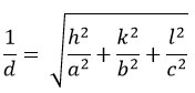
Here (hkl) represents the miller indices values, and d represents interatomic distance. The lattice parameters were found to be a = 0.5436 nm and c = 1.0856 nm, these are coincidences with the published data25 and JCPDS card No. 26-0575. Additionally, the c/a ratio is ~ 2, confirming the film structure as kesterite. The crystallite size (D) was computed using the Debye-Scherrer formula
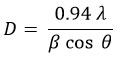
Here λ, β, and θ denote the wavelength of the X-rays, the full width at half maximum, and Bragg’s angle correspondingly. The obtained crystallite size of the Cu2ZnSnS4 thin films grown in two different conditions was tabulated in Table 2. The crystallinity improved when the films were allowed to remain on the hot plate for 15 minutes following deposition, as opposed to immediate extraction. XRD studies confirm that the films’ crystallinity was notably influenced by the experimental conditions. The dislocation density of the films (δ = 1/D2) as well as the number of crystallites (N = t/D3) in the deposited films were computed and tabulated in Table 2. These results confirm that the dislocation density and microstrain in the Cu2ZnSnS4 thin films declined when the films were left on the hot plate for 15 minutes after the spray pyrolysis. This concludes that the crystallinity of films that were improved when the films were subjected to post-experimental heating on the hot plate about 15 minutes, before extraction of the films.
 |
Figure 1: XRD spectra of the Cu2ZnSnS4 thin films (a) extracted immediately from the hot substrate after spray deposition (b) extracted from the hot substrate for 15 minutes after spray deposition |
Table 2: Cu2ZnSnS4 thin films crystallite size (D), dislocation density (δ), number of crystallites (N), Microstrain (ε) values.
|
Type of film |
D nm |
δ 10-3 nm-2 |
N 1016 m-2 |
ε 10-3 |
|
Immediately extracted |
18.2 |
3.019 |
7.464 |
1.599 |
|
Extracted after 15 min. of deposition |
23.3 |
1.842 |
3.558 |
1.563 |
Fig. 2 depicts the typical micro-Raman spectrum of the Cu2ZnSnS4 thin film. These films were subjected to a 15-minute treatment on a hot plate after the deposition process before being extracted. The obtained micro-Raman spectrum exhibits a predominant peak at 336 cm-1 as well as a low intense mode at 293 cm-1 confirming the existence of a kesterite structure. This observation is consistent with the X-ray diffraction results.
 |
Figure 2: Raman spectrum of the Cu2ZnSnS4 thin films extracted from the hot substrate for 15 minutes after spray deposition |
Fig. 3 shows the typical X-ray photoemission spectra of Cu2ZnSnS4 thin films extracted from the hot substrate for 15 minutes after spray deposition. The peak position values are tabulated in Table 3. The reported values26 and the attained peak values are in good coincidence.
 |
Figure 3: X-ray photoemission spectra of Cu2ZnSnS4 thin films extracted from the hot substrate for 15 minutes after spray deposition |
Table 3: Binding energies of CZTS thin films in XPS spectrum
|
Peaks’ binding energies (eV) |
|||||||
|
Cu |
Zn |
Sn |
S |
||||
|
2p3/2 |
2p1/2 |
2p3/2 |
2p1/2 |
3d5/2 |
3d3/2 |
2p3/2 |
2p1/2 |
|
932.5 |
952.2 |
1021.9 |
1045.7 |
487.1 |
495.1 |
161.7 |
162.7 |
SEM analysis
Maintaining a fine surface morphology is a crucial factor in thin film solar cells. The Cu2ZnSnS4 thin film SEM images captured under two distinct experimental conditions was displayed in Fig. 4. The SEM image confirms the improvement in the grains with the collection of the sample time from the hot substrates. On the surface of the film, the grains were firmly packed and evenly spaced when these were kept on the hot plate for 15 minutes after the pyrolysis. These dense morphologies offer advantages for solar cells27.
 |
Figure 4: SEM image of the Cu2ZnSnS4 thin films (a) extracted immediately from the hot substrate after spray deposition (b) extracted from the hot substrate for 15 minutes after spray deposition |
Optical analysis
The spectral transmittance curves were shown in Fig. 5. α = ln expression was used to get the optical absorption coefficient (α) value, where t, R and T correspond to the film thickness, reflectance, and transmittance, respectively11. Fig. 6 shows the optical absorption coefficient Vs photon energy for Cu2ZnSnS4 films, which were left on the hot plate for 15 minutes after the pyrolysis. This value was found to be more than 104 /cm. The material band gap was calculated by using a mathematical expression: αhν = A(hν-Eg)n, with h representing Planck’s constant, ν signifying the incident radiation frequency, and A denoting a constant. This equation satisfied when n = ½, affirming the presence of direct allowed transitions in the material11.
 |
Figure 5: Spectral transmittance curve of Cu2ZnSnS4 thin films (a) extracted immediately from the hot substrate, (b) extracted from the hot substrate for 15 minutes after spray deposition |
 |
Figure 6: Optical absorption coefficient of Cu2ZnSnS4 thin film extracted from the hot substrate for 15 minutes after spray deposition |
Fig. 7 illustrates the Tauc curves for deposited thin films. By examining the intercepts on the hν-axis, the energy band gaps of Cu2ZnSnS4 films were determined to be 1.52 eV and 1.50 eV6,25. It was observed that the energy band gap was slightly decreased when the films were subjected to 15 minutes of post-spray pyrolysis treatment on a hot plate, indicating an enhancement in film crystallinity. This optical analysis outcome coincided with X-ray diffraction studies. In general, a higher degree of crystallinity leads to a narrower range of energy levels. Consequently, the energy required to promote electrons from the valence band to the conduction band decreases, resulting in a reduced energy band gap. The measured band gap value closely approached the optimal band gap, which is necessary to achieve the highest theoretically attainable photovoltaic conversion efficiency.
It was observed that small cracks were noticed in the deposited films when these were kept on the hot plate for 30 minutes after the completion of spray pyrolysis and were later extracted.
 |
Figure 7: (αhν)2 versus hν of Cu2ZnSnS4 thin films (a) extracted immediately from the hot substrate, (b) extracted from the hot substrate for 15 minutes after spray deposition. |
Four-probe method was used to evaluate the room-temperature electrical studies of Cu2ZnSnS4 films. The conductivity of these films was measured to fall in the range of 1.39 x 10⁻² – 1.52 x 10⁻² (Ωcm)-1. Employing the hot probe technique, the conductivity of the films was found to be p-type6,9.
Device properties
A typical solar cell made up of Cu2ZnSnS4 thin film was left on the heated substrates for 15 minutes after the spray pyrolysis. The Cu2ZnSnS4 solar cell was fabricated with glass/Mo/Cu2ZnSnS4/CdS/Au layering sequence. Chemical bath deposition has been utilized to deposit CdS thin films at 60 °C24, which have been utilized as a buffer layer. A metallurgical connection between the Cu2ZnSnS4/CdS thin films was established by annealing them at 140 °C for approximately 10 minutes within a vacuum furnace. Ultimately, the top contact was established using Au metal to establish a metallic connection. The J-V performance of the CZTS solar cell is shown in Fig.8. The resulting solar cell had an open circuit voltage of 495 mV and a short circuit current of 3.38 mA/cm2. These cells exhibited a Fill Factor of 0.52 and an efficiency of 0.47%. The low performance of the cell might be due to non-optimization of electrical studies of the absorber layer and buffer layer of the films. In addition to these layer thicknesses, junction properties are also one of the reasons. However, solar cells produced via chemical synthesis exhibited low efficiency, potentially attributed to suboptimal film thickness and the presence of minor impurity phases in an amorphous state28. Ongoing studies are addressing these issues.
 |
Figure 8: J-V characteristics of CZTS solar cell. |
Conclusion
Cu2ZnSnS4 thin films are successfully developed at an optimized chemical spray pyrolysis process. The films are grown at a substrate temperature of 370 °C. The deposited films were kept on a hot plate for 15 minutes, significantly influencing the crystallinity of the films. These films exhibit a kesterite structure, with their lattice parameters determined as follows: a = 0.5436 nm and c = 1.0856 nm. The band gaps of these films are found to be 1.50 eV, which is comparable to the optical conversion in photovoltaic applications. Furthermore, the films display p-type conductivity. The thin film heterojunction solar cell constructed from Cu2ZnSnS4 exhibited an efficiency of about 0.5%.
Acknowledgment
The authors are extremely thankful to the University Grants Commission (UGC), New Delhi for providing the experimental setup to carry out this research work
Conflict of interest
The author states that the publication of this work does not present a conflict of interest.
References
- Krishna, K.G.; Kanak, K.; Ranjan K.G.; Manickam, R.; Xiao-Zhi, G., Energies, 2021, 14(4), 1122.
CrossRef - Marino, C.; Block, T.; Pottgen, R.; Villevieille, C., J. Power Sources, 2012, 342, 616-622.
CrossRef - Nagamalleswari, D.; Kumar, Y.B.K.; Ganesh, V., Physica B: Physics of Condensed Matt., 2021, 616, 413119.
CrossRef - Sobayel, K.; Shahinuzzaman, M.; Amin N.; Karim, M.R.; Dar, M.A.; Gul, R; Alghoul, M.A.; Sopian, K.; Hasan, A.K.M., Akhtaruzzaman, Md., Solar Energy, 2020, 207, 479-485.
CrossRef - Shin, T.; Mitsutaro, U.; Masaki, H.; Takahiro, M.; Tadayoshi, I; Prog. Photovoltaics Res. Appl., 2017, 25, 14–22.
- Hironori, K; Kotoe, S.; Tsukasa, W., Hiroyuki, S.; Tomomi, K.; Shinsuke, M., Sol. Energy Mater. Sol. Cells. 2001, 65, 141-148.
- Zakaria, O.E.; Mohammed, A.; Khakan, A.E., Nanomaterials, 2020, 10, 1393–1393.
CrossRef - Akcay, N.; Ataser, T.; Ozen, Y.; Ozcelik, S., Thin Solid Films, 2020, 704, 138028.
CrossRef - Jayasree, Y., Kumar, Y.B.K.; Babu, G.S.; Bhaskar, P.U., Physics B: Condensed Matter, 2021, 618, 413199.
CrossRef - Macías-Cabrera, CA.; Campos-Álvarez, J.; Gamboa, S.A.; Aguilar-Martínez, J.A.; Peña-Méndez, Y, Materials Today: Proceedings, 2021, 46, 3109–3113.
CrossRef - Nagamalleswari, D.; Kumar, YBK.; Kiran, Y.B., Babu, S.G., Energy sources, Part A: Recovery, Utilization and Environmental Effects, 2019, 41, 3001-3012.
CrossRef - Ahmoum, H.; Chelvanathan, P.; Su’ait, M.S.; Boughrara, M.; Li. G., Al-Waeli, AHA.; Sopian, K.; Kerouad, M.; Amin.N, Superlattices and Microstructures, 2020, 140, 106452.
CrossRef - Arslan, A., Jolly, J.; Bano, N.; Ajaz, M.; Un, N.; Ali, A.; Ahmad, W.; Mahmood, K.; Arshad, M.I.; Salma, I.; Rehman, U.; Amin, N.; Hussain, S., Ceramics International, 2019, 45, 10876–10881.
CrossRef - Jeganath, K.; Sajan, D.G.; Murari, M.S.; Raviprakash, Y., Materials Letters, 2021, 300, 130168.
CrossRef - Kumar, K.B.Y; Bhaskar, P.U., Gandam, S.B.; Raja, V.S., Phys. Status Solidi A, 2010, 207, 149-156.
CrossRef - Reddy, V.R.M.; Mohan, R.P.; Guddeti, P.R.; Gedi, S.; Reddy, K.K.Y.B.; Babu, P.; Kim, W.K.; Kote, T.R.R., Park, C., J. Industrial and Engineering Chemistry, 2019, 76, 39-74.
CrossRef - Kumar, K.B.Y.; Babu, G.S.; Chalapathi, U.; Kiran, Y.B.; Bhaskar, P.U.; Park, S.; Physica B: Condensed Matter, 2023, 670, 415366.
CrossRef - Kumar, K.B.Y.; Doddipalli, R.R.; Nagamalleswari, D.; Tarigonda, H., SAE Technical Paper, 2022, 28-0573.
- Nagamalleswari, D.; Kishorekumar, Y.B.; Kiran, Y.B.; Gandam, S.B., Chalcogenide Letters, 2020, 17, 505-513.
CrossRef - Kumar, Y.B; Suresh, B.G.; Uday, P.B., Raja, V.S., Sol. Energy Mater. Sol. Cells. 2009, 93, 1230-1237.
CrossRef - Kishorekumar, Y.B.; Babu, S.G.; Uday, P.B., Raja, V.S., Physica Status Solidi A, 2009, 206:1525-1530.
CrossRef - Kumar, Y.B.K.; Nagamalleswari, D.; Babu, S.G., Physics B: Condensed Matter, 2022, 45, 414263.
CrossRef - Nagamalleswari, D.; Kumar, Y.B., Indian J. Science and Technology, 2022, 15, 1399-1405.
CrossRef - Kumar, Y.B.K.; Raja, V.S., Surfaces and Interfaces, 2017, 9, 233-237.
CrossRef - Vigil-Galan, O.; Rodríguez, E.M.; Maykel, C.; Fontané, X.; Sylla, D.; Roca, I.; Fairbrother, A.; Saucedo.; Pérez-Rodríguez. A., Sol. Energy Mater. Sol. Cells, 2013, 117, 246-250.
CrossRef - Hurtado, M.; Cruz, S.D.; Becerra, R.A.; Calder′on, C.; Bartolo-P′erez, P.; Gordillo, G.; 2014, Proc. IEEE, 368–372.
- Rajeshmon, V.G.; Vijayakumar, K.P.; Kartha, C.S., J. Physics: Conference Series, 2019, 1461, 15-19.
CrossRef - Vigil-Galán, O., Maykel, C.; Rodríguez, M.; Jiménez-Olarte, D.; Aguilar-Frutis. M.; Saucedo, E.; Solar Energy Materials & Solar Cells, 2015, 132, 557-562.
CrossRef

This work is licensed under a Creative Commons Attribution 4.0 International License.
About The Author
![]()
A New Edition of Web of Science
Journal Impact Factor
2022: 0.5
Five Year: 0.8
Journal is Indexed in

Cabells Whitelist
![]()


