Characterization of Platinum (Pt) Based Nanocomposite Thin films
S P Singh1 and U C Srivastava2
1Department of Physics, Swami Vivekanand Govt.P.G. College, Lohaghat, Champawat, Uttrakhand, India,
2Department of Physics, Amity Institute of Applied Sciences, Amity University, Noida-UP, India.
Corresponding Author E-mail: ucsrivastava@amity.edu
DOI : http://dx.doi.org/10.13005/ojc/390634
Article Received on : 06 Sep 2023
Article Accepted on :
Article Published : 10 Nov 2023
Reviewed by: Dr. Ali N. Sabbar
Second Review by: Dr. K. N. Houk
Final Approval by: Dr. B. K Sharma
In the present communication we are reporting experimentally observed data of Platinum (Pt) based nano composite thin films. Platinum (Pt) shows crystalline behavior whereas Antimony tri sulfide (Sb2S3) shows amorphous behavior, and it has layered structure. In this observation the ratio of Pt and Sb2S3 is taken in 1:10 respectively, due to which multiple peaks shown in X-ray Diffraction (XRD) and have studied its variation by doing UV-VIS spectroscopy of different thickness of deposited material. Therefore, by this analysis of the nano composite materials we can synthesize nanomaterials which have great applications in photodetectors, solar cells, drug delivery, Fuel Cell, sensors, bioimaging and many other materials fabrications.
KEYWORDS:Nanoparticles; Nanostructures; Pt NP; SEM; Thin film; Vapor deposition; XRD analysis
Download this article as:| Copy the following to cite this article: Singh S. P, Srivastava U. C. Characterization of Platinum (Pt) Based Nanocomposite Thin films. Orient J Chem 2023;39(6). |
| Copy the following to cite this URL: Singh S. P, Srivastava U. C. Characterization of Platinum (Pt) Based Nanocomposite Thin films. Orient J Chem 2023;39(6). Available from: https://bit.ly/3Gd0XQh |
Introduction
Deposition of these thin films is done by both physical techniques as vapour statement, sputtering and laser removal and chemical processes as a spray pyrolysis, sol-gel and chemical vapour deposition and there are numerous other electrochemical strategies which are utilized as a part of the deposition of the film 1,8. The films were formed by physical vapor deposition method thus there was no reaction takes place in its chemical analysis. It is most used physical deposition. The materials used here for our study are Platinum (Pt)and Antimony tri sulfide (Sb2S3). both samples are taken in 1:10 proportions where Platinum (Pt) is 1x and Sb2S3 is 10x because of which the crystalline part of Pt is quite small because of which sharp peaks was not discover insist multiple peaks with distortion occur 2. These two samples of Pt and Sb2S3 were taken in pallet form from which small part of this pallet is taken in the deposition process and after that some little amount of this material taken in the tungsten boat to determine the number of nanoparticles deposited on the glass substrate 3,4. Along these lines for discovering better properties of sample taken, the amount of material is taken in appropriate amount so that it is deposited on the substrate with great film thickness 5.
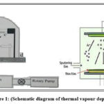 |
Figure 1: (Schematic diagram of thermal vapour deposition) |
Experimental details
In this analysis we have study the Optical properties when Pt (Platinum) nanocrystals dispersed in amorphous Sb2S3 matrix. First, we prepare a pellet of Pt & Sb2S3 at 4 ton of pressure. For the analysis of thin film, we used physical vapour deposition technique 6,7. After deposition is occur on the glass slide, we analyze the XRD, UV-VIS spectroscopy and SEM of the composite film material deposited. From the SEM, we can see the surface morphology and can determine the vertical view of prepared thin films 6. We thus doing these procedures we analyze the data from which the properties of the material used is found out and compare with ASTM and JCPDS standard of the material 7,8. I have taken Platinum (Pt) and Antimony tri sulfide (Sb2S3). Samples are taken in to 1:10 ratio i.e. Antimony tri sulfide (Sb2S3 ) – 2.002 grams & Platinum (Pt) -0.202 grams. we have prepared samples with the help of pressure pelletizer by applying 4 ton of pressure on mix powdered form of Platinum and antimony tri sulfide. After this process we got a solid pellet form of Pt and Sb2S3. Now we must analyze the properties of composite thin films of Pt in Sb2S3.
After deposition the film is taken to analyze XRD, UV–V is spectroscopy, to see surface morphology by SEM and find the band gap of the deposited film composite material.
 |
Figure 2: Material deposited on the film. |
 |
Figure 3: Deposited film used after thermal vapour deposition |
The colour of the thin film vary. It is depending upon the amount of material used during the physical vapour deposition process 9,10. Generally, the colour of the deposited film is yellow to brownish orange. These glass slides are obtained through physical deposition method and these glass slides are used for analysis purpose. After formation of the graph, the grain size of the material is used to calculate from the collected data and analysis of the generated data is done by using the origin software at which the value of grain sizes by fitting of Lorentzian data. In the X-rays diffractometer after the solar slits the x-rays goes to mono – chromator and receive at the detector.
Computations
The data received at the detector is then analyze by using the software and the collected data use to find the variation of 2Ѳ with intensity. These all data are generally used for Structural analysis and to find the particle size of the material used but here as amorphous (Sb2S3) is in large quantity therefore the amount of material (Pt) for scattering is not sufficient 11.
 |
Figure 4: Graph 1: XRD graph of sample (1). |
 |
Figure 5: Graph 2 : Lorentzian fit of sample (1). |
 |
Figure 6: Graph 3 : XRD graph. |
 |
Figure 7: Graph 4 : Lorentzian fit of sample (2). |
 |
Figure 8: Graph 5 : XRD graph. |
 |
Figure 9: Graph 6 : Lorentzian fit of sample (3). |
The above graphs are showing the variation of 2Ѳ with the Intensity in which multiple numbers of peaks are shown this is just because of the majority of amorphous material present in it, the data for multiple peaks by selecting the few peaks and doing Lorentzian fit for multiple peaks. UV-VIS is used in visible and adjacent (near UV and IR) ranges 12. The sorts of signs shaped where the electron shaft encroaches on an example surface including auxiliary electrons, back – scattered electrons, twist drill electrons, attributes x – beams and photons of various energies. These signs are delivered from a specific discharge volume within the specimens and are utilized to decide the creation, surface morphology, surface geography. The sharpness and complexity of SEM micrographs and profundity of field in pictures are reliant upon three electron pillar parameters.
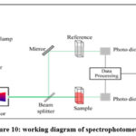 |
Figure 10: working diagram of spectrophotometer. |
At the point when test size and edge of union are made little then test current will be decreased 13. We can pick up a little pillar edge by utilizing a little target lens gap, a long working separation or both. In this way, these parameters must be chosen in a way to accomplish reasonable imaging conditions in every circumstance. Since the picture is delivered by optional outflow of electrons, the examples ought to direct. Be that as it may, we can examine the surface of non – leading in the wake of covering of a gold/platinum film on the specimen. The thickness of the gold coat is regularly utilized as 500 to this auto fine coater used in the coating of platinum on thin fills before Scanning electron microscopy. This coater, which comprises of a primary main unit and a pump, is expected primarily to get ready examples (specimen) for SEM perception. It coats organic and other nonconductive examples (specimens) with metals, proficiently and in a brief timeframe. These all are the graphs of UV visible spectroscopy. UV visible spectroscopy is done by double beam Spectrophotometer. All graphs show the different lines, the same straight line which is parallel to wavelength axis i.e the value of wavelength is constant up to some extent and after that extent the value of wavelength is decreasing non uniformly.
 |
Figure 11: Graph 1.1 : UV analysis of sample 1 |
 |
Figure 12: Graph 1.2 : UV analysis of sample 2 |
 |
Figure 13: Graph 1.3: UV analysis of sample 3 |
The XRD graphs are having multiple number of peaks which shows the amorphous behaviour of Sb2S3. The graph of XRD is in between Intensity and 2Ѳ (2Theta). When we draw the Lorentzian single fit of this then the Lorentzian single fit is occurring just below the peaks 14.
Result and Analysis
We have used the software origin 8.0 for data analysis and finding the band gap of the samples with the help of film thickness and the wavelength, ln I/ I0, alpha, energy and the band gap is calculated by plotting the graph between energy and intensity. We have also done the UV visible analysis and X-ray diffraction (XRD) analysis graphs and Lorentzian fitting. We have calculated the particle size of XRD data, Image analysis in Scanning electron microscopy (SEM) is done using XT microscope control software and SEM is done by using FEI Quanta 200 F instrument 15,16. After this, we have calculated the particle size of round shape view in SEM images by applying some basic mathematical formulation.
 |
Figure 14: Sample 1 ( SEM Image). |
 |
Figure 15: sample 2 ( SEM image). |
 |
Figure 16: sample 3 ( SEM image) |
The scanning electron microscopy of the sample 1 ,2 and 3 i.e. Surface morphology. As you can see in the images that these images are showing some different shapes. Now we will calculate the particle size of these round shapes presents in the images and after that we will find its average particle size 17,18. Avg. particle size of sample 1:- 0.046839754 microns = 46.839754 nm. Avg. particle size of sample 3:- 0.46545736 microns = 465.45736 nm.
Table 1 : Calculation of particle size of XRD
|
S.NO. |
Centre (2Ѳ) |
Width (β) |
Particle size (D) (A0) |
|
1 |
29.462 |
0.2134 |
382.54 |
|
2 |
43.457 |
0.2440 |
356.37 |
|
3 |
47.054 |
0.2421 |
365.44 |
|
4 |
29.446 |
0.2065 |
405.44 |
|
5 |
47.002 |
0.3177 |
274.70 |
|
6 |
54.548 |
0.3863 |
235.40 |
|
7 |
29.461 |
0.1560 |
536.42 |
|
8 |
30.009 |
4.5767 |
22.44 |
|
9 |
38.352 |
0.0060 |
14142.42 |
Table 2 : Particle Size analysis.
|
S.NO |
Particle size of sample 2 |
Particle size of sample 3 |
|
1 |
0.0055379 |
0.1020539 |
|
2 |
0.0451895 |
0.1253950 |
|
3 |
0.0903935 |
0.1530612 |
|
4 |
0.0437434 |
0.3163075 |
|
5 |
0.0495670 |
0.1151661 |
|
6 |
0.0553950 |
0.2046787 |
|
7 |
0.0189518 |
0.2420072 |
|
8 |
0.0065568 |
1.3848425 |
|
9 |
0.0787186 |
1.2973760 |
|
10 |
0.074344 |
0.7142857 |
Conclusion
Pt is the best noble metal which gives very promising results when used as electrocatalyst for applications as electrode in alkaline Fuel Cells, photoelectrode in dye sensitized solar cell etc. The multiple peaks in samples are discovered in the UV-VISIBLE absorption spectrum of Sb2S3 films, having Ag dispersed in it because of which there is occurrence of surface plasmon resonance (SPR) phenomena. In UV visible spectroscopy, as we can see all graphs are showing the same straight line which is parallel to wavelength axis i.e. the value of wavelength is constant up to some extent and after that extent the value of wavelength is decreasing non uniformly. Similarly, when we measure the band gap energy with time then this shows the ageing effect of the deposition. In X-ray diffraction, as we can see all graphs are showing the different peaks 19,22. Formation of these peaks showing the presence of silver in the sample i.e., crystalline in nature. Scanning electron microscope (SEM) images are showing the formation of different shapes in it i.e., different surface morphology. Pt composites with non-noble metals, polymers, and carbon nanomaterials, with a view to get the final product giving better efficiency than pure Pt. Emphasis is also on for using very little of Pt in the composite 23,24.
Acknowledgment
The authors pay his gratitude to Uttarakhand University, NPL-New Delhi, ,Roorkee University for their various technical support and using the lab facilities for data analysis and sample preparation.
Conflict of interest
The authors has no conflict of interest.
References
- Moores, A.; Goettmann, F. New J. Chem. 2006,30 ,1121–32.
- Tilaki ,R. M.; Irajizad ,A.; Mahdavi, S. M. Applied Physics A. 2006,84, 215.
- Fang, N.; Lee, H.; Sun, C.; Zhang, X. Science. 2005,308, 534.
- Bian, X.J.;Lu, X.F.; Jin, E.; Kong, L.R.; Zhang, W.J.; Wang, C. Talanta .2010, 81(3), 813-818.
- Kim, J.; Choi, H.; Nahm, C.; Park, B. Electron. Mater. Lett. 2012,8, 351–64.
- Anlian ,P.; Zhiping, Y.; Huagui, Z.; Fangxing, L.; Yongchun, Z.; Xiaobo, S.; Zejun, D. Appl. Surf. Sci. 2003,205, 323–8.
- Singh, B. K.; Shefer, E.; Breskin, A.; Chechik, R.; Avraham, N. Nucl. Instrum. Methods Phys.Res. A .2000,454, 364–78.
- John, L.; Vossen.; Werner, Kern. Thin Film Processes II. Boston. Academic Press. 1991.
- Kong ,L.; Joly, A. G.; Droubay, T. C.; Gong, Y.; Hess, W. P. Appl. Phys. Lett. 2014,104, 171106
- Dobrzanska.; Danikiewicz, A.D.; Kukowiec, D. Phys. Stat. Sol. B. 2013,250(12),1-6.
- John, F.O’Hanlon. AUser’s Guide to Vacuum Technology. John Wiley & Sons. Inc. 1st Edition.2003.
- Mattox, D.M. Handbook of Physical Vapor Deposition (PVD) Processing. William Andrew Publishing/Noyes, 1st edition. 1998, 2nd edition. 2003.
- James, M. Lafferty. Physics Today.1981,34,11,211-31.
- Jayaprakash, J.; Michael, T. A Student’s Handbook Postek.1980.
- Lyman, C. Springer. Scanning Electron Microscopy, X-Ray Microanalysis, and Analytical Electron Microscopy Workbook,1990.
- Ueno, K.; Juodkazis, S.; Mino, M.; Mizeikis, V.; Misawa, H. J. Phys. Chem. C. 2007, 111, 4180-4
- Hu, J .Q . Adv. Funct. Mater. 2004,14, 183.
- Choi, B. H; Lee,H. H; Jin, S; Chu, S; Kim, S. H. Nanotechnology. 2007,18, 075706.
- He, G.; Yang, S.; Liu, K.; Walter, A.; Chen, S.; Chen, S. ACS Catal. 2013,3, 831-838.
- Hui, M.; Zhan, Y.; Zeng, D.; Zhang, X.; Zhang, G.; Jaouen, F. Nano Micro Small. 2015,11(27), 3377-3386.
- Li, L.; Chow, W.; Wong, W.; Chui, C; Wong, R.S. Journal of Organometal. Chem. 2011,696(6),1189-1197.
- Srivastava, U.C. Johnson Matthey Technol. Rev. 2021, 65, (1), 87-93.
- Isaac, Nandgavkar. M. S.; Sharon, M. Advances in Materials Research. 2017, 6, 2, 129-153.
- Srivastava ,U.C.International Journal of Modern Physics B. 2016,30,1750020-28.

This work is licensed under a Creative Commons Attribution 4.0 International License.
About The Author
![]()
A New Edition of Web of Science
Journal Impact Factor
2022: 0.5
Five Year: 0.8
Journal is Indexed in

Cabells Whitelist
![]()


