Impact of Sb Incorporation on the Structural and Optical Properties of CZTS Thin Films Grown by Spin Coating Technique
Jagdish Prasad1,2* , Jagavendra Yadav1, Sunil Kumar1, Hansraj Sharma1 and Mangej Singh1
1Department of Physics, University of Rajasthan, Jaipur, Rajasthan, India.
2Department of Physics, Govt. Science College, Sikar, Rajasthan, India.
Corresponding Author E-mail: jpdhaka22@gmail.com
DOI : http://dx.doi.org/10.13005/ojc/390308
Article Received on : 13 Mar 2023
Article Accepted on :
Article Published : 15 May 2023
Undoped and Sb-doped, Cu2ZnSnS4 (CZTS) thin films have been synthesized on ordinary glass slides using the sol-gel spin coating method. The effect of variation in Sb doping concentration on structural, optical, and surface morphological characteristics of CZTS thin films has been investigated. The XRD analysis reported that these samples show a kesterite phase which is further confirmed by Raman spectra. The crystallite size for CZTS thin film samples increases from about 9 nm to 15 nm. The surface morphology of CZTS thin films has been investigated by SEM analysis. The chemical composition of existing elements has been presented by EDS analysis. The optical properties have been examined by UV-Vis spectrometer. For synthesized thin films energy band gap values vary from 1.90 eV to 1.62 eV and the refractive index varies from 2.74 to 2.85. Additionally, the high-frequency dielectric constant (ε∞) and static dielectric constant (ε0) values have been determined.
KEYWORDS:CZTS thin film; Kesterite Phase; optical properties; Sol-gel; spin coating; Sb-doping
Download this article as:| Copy the following to cite this article: Prasad J, Yadav J, Kumar S, Sharma H, Singh M. Impact of Sb Incorporation on the Structural and Optical Properties of CZTS Thin Films Grown by Spin Coating Technique. Orient J Chem 2023;39(3). |
| Copy the following to cite this URL: Prasad J, Yadav J, Kumar S, Sharma H, Singh M. Impact of Sb Incorporation on the Structural and Optical Properties of CZTS Thin Films Grown by Spin Coating Technique. Orient J Chem 2023;39(3). Available from: https://bit.ly/41GtK7U |
Introduction
Alternative energy sources are available to meet the global need for energy, with solar energy being the best choice [1]. Thus, it is essential to discover such environmentally acceptable, affordable, and readily accessible semiconductor materials for the manufacturing of solar cells. Silicon is utilized as a semiconductor material in silicon solar cells, which are the first-generation photovoltaic cells. Although such solar cells have significant power conversion efficiency, they also have several disadvantages, including overpriced, a small absorption coefficient, and a lack of silicon in the natural world. Copper Indium Selenide (CIS), Cadmium Telluride (CdTe), and Copper Indium Gallium Selenide (CIGS) are utilized as semiconductor materials in the second-generation photovoltaic cells, which are referred to as thin-film solar cells. CIGS photovoltaic cells are high power conversion efficient of over 20% efficiency [2-9]. On the other hand, In and Ga are not abundant on Earth, hence the presence of these elements makes large-scale commercial manufacture of CIGS solar cells more problematic [10]. It is critical to investigate developing an alternate absorber material to tackle the problem of high cost and scarcity. Copper Zinc Tin Sulphide (CZTS) could be considered a potential component for thin film solar cells as a consequence of its numerous advantages such as it is made up of cheaper, earth-abundant, and non-hazardous elements, as well as an absorber layer with a high absorption coefficient (104 cm-1) and a wide energy band gap 1.4-1.5 eV which is fitted with ideal energy band gap for thin film solar cells [11-13]. CZTS is a quaternary compound containing a large number of impurities and defects compared to ternary and binary compounds, which have a direct impact on charge generation, charge separation, and electron-hole pair recombination [14-15]. On this basis, the formation of single-phase CZTS material with larger grain sizes is critical to enhancing device characteristics [16]. As a result, research on CZTS thin films is ongoing to enhance the characteristics of these thin films. The incorporation of alkali metals in CIGS and CZTS absorber layers described an improvement in the thin film’s grain size, surface morphology, electrical, and optical characteristics. Hence, the device’s performance was improved [17-25]. Although numerous new studies on the integration of Li, Rb, and Cs alkaline elements were reported in recent years, most of the investigations have concentrated on Na incorporation [26-30]. In earlier research, CuIn1xGaxSe2ySe (CIGS) photovoltaic cells are manufactured at low temperatures (400 °C) utilizing the Sb-doping approach, with the absorber films being deposited using a hydrazine-based procedure. It was discovered that utilizing cross-sectional SEM, Sb-induced grain size enlargement was notable at these relatively low processing temperatures. These Sb-doped samples showed an enhancement in the efficiency of approximately 2-3% over their Sb-free sister counterparts [31]. It studied the optical and electrical characteristics of cation (Sb, Al, Ga, Ba) incorporated CZTS/Se materials, in which Sb and Ba have lower formation energies than Al and Ga. Additionally, the bulk modulus of the Sb substitute (65/51.25 GPa) with pure CZTS/ Se (65.8/53 GPa) shows its suitability as a dopant. The obtained results show that the Sb-doped CZTS/Se is an ideal candidate for use as a component in relatively high-efficiency solar cells due to its reduced formation energy, preferred energy gap, and outstanding optical absorption [32]. Quantum mechanical investigations on Sb incorporated CZTS thin films revealed that Sb prefers to replace Sn atomic positions. Due to Sb incorporation, a half-filled intermediate band is formed by the Sb 5s states at 0.5 eV over the valence band maxima. It may help improve the photocurrent and enhance the efficiency of photovoltaic cells [33].
In this study, we synthesized Sb-doped CZTS thin films using a spin coating technique with various doping concentrations in the ratio of Sb/Cu(w%) = 0%, 5%, 10%, and 15%. Thus, we used Sb as a dopant with low and high doping concentrations. Hence we have investigated the impact of variation in Sb doping concentration on the structural, surface morphological and optical characteristics of CZTS thin films.
Materials and methods
Preparation of a sol-gel precursor
Step-I: Initially, 0.030 M of CuCl2.2H2O and 0.015 M of ZnCl2 were dissolved into 50 mL of 2-Methoxy ethanol and the solution was put on a magnetic stirrer with a hot plate at 50 °C for 30 minutes. Then 0.015 M of SnCl2.2H2O and 0.120 M of thiourea (SC (NH2)2) were added to the above solution and finally, 30 drops of monoethanolamine (MEA) were added to the aforementioned solution, which aids in the complete dissolution of the metal salts. After one hour of magnetic stirring at 50 °C on a hot plate, a transparent yellow solution was achieved.
Step-II: Antimony (III) acetate (Sb(OAC)3) was added to the above solution. Thus four types of precursors solution were formed with a weight percentage of Sb/Cu (w%) = 0%, 5%, 10%, and 15%, and named S0, S5, S10, and S15 respectively.
Fabrication of CZTS thin film
Firstly the glass slides were cleaned via isopropyl alcohol, acetone, and distilled water respectively. Then, the precursor solution was spin-coated at 2500 rpm on a cleaned glass slide; a thin film-coated glass slide was put on a hot plate for 5 minutes at 100°C. To obtain the thin films of the appropriate thickness, this operation was repeated 3 to 4 times. These thin films were then annealed for 10 minutes at 350°C in the air. This thin film fabrication process was operated for S0, S5, S10, and S15 solutions.
Characterization Techniques
Different approaches were used to analyze the CZTS thin films. An X-ray diffraction spectroscopy (XRD; Panalytical X Pert Pro using CuKα radiation) was used to determine the crystal structure of the Sb-doped thin films. A field emission scanning electron microscopy (FESEM) was used to determine the elemental composition (Nova Nano FE-SEM 450). A UV-Vis spectrophotometer (LAMBDA 750 Perkin Elmer) was used to calculate the optical properties of Cu2ZnSnS4 thin films in the 200-800 nm wavelength range. Raman spectroscopy (STR 500 CONFOCAL MICRO) was used to get the Raman spectra at ambient temperature. The 532 nmwavelength emission line of an Argon ion laser was used to capture these Raman spectra. Surface morphology was analyzed using a ZEISS scanning electron microscopy (SEM).
Results and Discussion
Structural properties
The XRD patterns of samples S0, S5, S10, and S15, are displayed in Fig. 1(b). The diffraction maxima occur in the neighbourhood of angles 2θ equal to 28.58˚, 47.45˚, and 56.16˚, which are compatible with diffraction at the planes (112), (220), and (312) respectively. The kesterite CZTS phase is confirmed by the development of these peaks. The JCPDS # 26-0575 card is in agreement with this [34]. These XRD spectra show that the diffraction angle for doped samples shifts to smaller values as compared to the undoped sample. The decrease in diffraction angle describes the increment in lattice constant which demonstrates the inclusion of Sb into the CZTS lattice. These doped Sb atoms tended to occupy Cu vacancies [35]. Table 1 shows the diffraction details at the plane (112) of Cu2ZnSnS4 thin films for various Sb doping levels. It has been noted that by raising the level of Sb doping, the FWHM of the plane (112) decreases which shows that the crystallinity has enhanced. Also, the I(112)/I(220) ratio for sample S15 is larger compared to other samples. It shows that 15 w% Sb doping aids (112) the favored orientation of CZTS films, which promotes crystalline growth [36-37]. The Debye–Scherer formula-
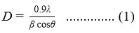
where λ = 1.54 Å and β is the full width at half maximum (FWHM); may be utilized to compute samples’ crystallite size D. The S0, S5, S10, and S15 samples have crystallite sizes of ̴ 9, 10, 11, and 15 nm, respectively. It also confirms that 15 w% Sb-doped CZTS thin films have better crystallinity in comparison to other Sb-doped as well as undoped films.
Table 1: The sample-specific data of FWHM ( β ), crystallite size (D), dislocation density (δ), strain (ε), and peaked intensity ratios of planes (112) and (220), for samples S0, S5, S10, and S15.
|
Sample |
β (112) |
D (nm) |
δ ×10-3 (nm-2) |
ε ×10-2 |
I(112) / I(220) |
|
S0 |
1.52 |
9.38 |
11.36 |
36.93 |
2.57 |
|
S5 |
1.37 |
10.46 |
9.13 |
33.11 |
2.17 |
|
S10 |
1.27 |
11.27 |
7.87 |
30.74 |
2.44 |
|
S15 |
0.98 |
14.58 |
4.70 |
23.77 |
4.07 |
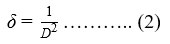
Furthermore, to obtain additional information regarding the defects in the CZTS thin films, we calculated the dislocation density and strain.
The dislocation density (δ) is given by the formula [38]-
while the strain is given by the relation [39]-
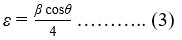
The values of β, D, δ, ε, and peaked intensity ratios of planes (112) and (220), are shown in Table 1. From Table 1, we conclude that crystallite size grows by the increment in Sb doping concentration, whereas FWHM, dislocation density, and strain diminish. Thus, for the enhancement in crystallinity of thin films; β, δ, and ε, should be lower and D should be greater. As a result, sample S15 exhibits better crystallization than the other samples.
Raman spectroscopy is a convenient technique for determining the phase of CZTS. Fig. 1(a) exhibits the Raman spectra for the samples. The samples S0, S5, S10 and S15, have their single intense peaks at ̴ 331 cm-1, 329 cm-1, 327 cm-1 and 326 cm-1 respectively. These peaks are assigned to the CZTS structure [40]. For all the samples Raman shifts are between 310 and 340 cm-1, which is attributed to the vibration of sulfur atoms [41]. The presence of only a single peak for each sample confirms the development of a single-phase CZTS thin film [42]. Also, the Raman spectra show that as Sb doping concentration increases, the intensity of Raman peaks changes. The Changes in the high-frequency dielectric constant are responsible for the variation in Raman intensity [43]. As demonstrated in Fig. 2, as the level of Sb doping rises, the Raman peak slightly shifts on the way to a lower wave number. As we know the radius of Sb+3 is larger than the radius of Cu+2. Hence force constant for the Sb-S bond is smaller as compared to that of the Cu-S bond. Thus decrease in the bond force constant causes red shifting of the Raman peak [44].
 |
Figure 1: (a) Raman spectra and (b) XRD spectra of undoped (S0) and doped samples (S5, S10, & S15). |
Elemental analysis and surface morphology
The elemental compositions of undoped and doped CZTS samples have been investigated by Energy Dispersive Spectroscopy (EDS). The EDS graphs (with inset tables) of the samples are displayed in Fig. 2(a,b,c,d). The inset tables show atomic and weight percentages of present elements. The EDS analysis verifies the presence of Cu, Zn, Sn, S, and dopant material (Sb), indicating that Sb doping concentration is maximum for the sample S15 (15 w%). The EDS graph for each sample shows a sharp intense peak of Si, which are because of the synthesis of CZTS thin films on the glass substrate.
The influence of Sb incorporation on surface morphological characteristics of CZTS thin film has been investigated by applying SEM. The SEM images of undoped and doped samples are displayed in the Fig. 3(a,b,c,d). The undoped sample S0 has a layer-type surface, in which no particle surface is identified. For the doped samples, (S5 and S10) the layer-type surface transforms into the particle-type surface. The sample S15 also shows a particle-type surface with increased grain size. Thus, by increasing Sb concentration crystallite size increases. The above findings match with the results of XRD.
 |
Figure 2: EDS graphs of (a) sample S0, (b) sample S5, (c) sample S10, and (d) sample S15. |
 |
Figure 3: SEM micrographs for (a) sample S0, (b) sample S5, (c) sample S10, and (d) sample S15 |
Optical properties
For the selection of good absorbing material for thin film solar cells, optical parameters like absorbance (A), transmittance (T), and band gap (Eg) are extremely important. We used a UV-Vis spectrophotometer to examine the optical characteristics of CZTS films. Fig 4(b) displays the graphs between % transmittance vs wavelength, for all the samples in the wavelength range 200-800 nm. These graphs show that transmittance is maximum around 700 nm, which is in the neighbourhood of the absorption edge of CZTS. It confirms the presence of a direct band gap in semiconducting materials. Fig 4(a) shows the graphs between absorbance vs wavelength, for all the samples. The absorption coefficient of a thin film can be calculated using the relation [45]:
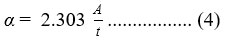
where A and t denote absorbance and thickness of the thin film, respectively. Tauc formula can be applied to calculate the optical band gap value of these samples [46]:
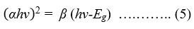
where β and Eg represent energy independent constant and band gap energy, respectively.
 |
Figure 4: (a) Absorbance vs. wavelength, (b) Transmittance vs. wavelength, and (c) (αhν)2 vs. (hν) graphs of CZTS thin film samples. |
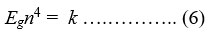
Fig 4(c) shows the graphs between hν and (αhν)2 , for all the samples. The intercept between the tangent {drawn to the graph between hν and (αhν)2 } and the axis provides the band gap value (Eg). The observed optical energy band gap value for the samples S0, S5, S10, and S15 are 1.90, 1.85, 1.71, and 1.62 eV, respectively. It concludes that by raising the Sb incorporation concentration, the energy band gap value of the CZTS thin film diminishes. According to reports, the quantum confinement effect causes the band gap to grow as the size of the crystal decreases. When a quantum dot’s dimension matches or exceeds the exciton Bohr radius, confinement occurs, and as the size decreases, the amount of electrons that can be held in a quantum dot increases substantially. Additionally, when the particle size decreases, the continuum in conduction and valence band that is seen in bulk materials is replaced with discrete atomic-like energy levels; hence band gap energy increases [47, 48]. Thus, the above finding matches with the results of XRD. The refractive index (n) of a semiconductor can be determined using the Moss equation [49, 50]
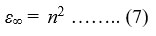
where k is a constant. The value of k is 108 eV [48, 49]. The optical high frequency dielectric constant (ε∞) may be determined by the equation:
where n is the refractive index [47]. The optical static dielectric constant (ε0) for CZTS thin films can be determined by the relation-
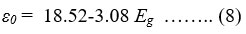
where, Eg is band gap energy [49, 50].
The calculated values of Eg, n, ε∞,and ε0, for CZTS films having various Sb incorporation concentrations are shown in Table 2.
Table 2: The values of optical energy band gap (Eg), refractive index (n), high-frequency dielectric constant (ε∞), and static dielectric constant (ε0) for samples S0, S5, S10, and S15.
|
Sample |
Eg (eV) |
n |
ε∞ |
ε0 |
|
S0 |
1.90 |
2.74 |
7.53 |
12.67 |
|
S5 |
1.85 |
2.76 |
7.64 |
12.82 |
|
S10 |
1.71 |
2.81 |
7.95 |
13.25 |
|
S15 |
1.62 |
2.85 |
8.12 |
13.53 |
Conclusion
The undoped and Sb-doped CZTS thin films were successfully fabricated by sol-gel spin coating technique on glass slides. We reported the impact of variation in Sb concentration on the structural, optical, and surface morphological characteristics of CZTS films. The XRD analysis shows the development of the kesterite phase in undoped as well as Sb-doped samples and we conclude that crystallite size grows by the increment in Sb doping concentration, whereas FWHM, dislocation density, and strain diminish. Thus, for the enhancement in crystallinity of thin films; β, δ, and ε, should be lower and D should be greater. As a result, sample S15 exhibits better crystallization than the other samples. Raman spectra show the presence of a single intense peak for each sample which confirms the development of single-phase CZTS thin film. These Raman peaks shift towards lower wave number with increment in Sb doping concentration. This red shifting of Raman peaks is due to a decrease in bond force constant by increasing Sb doping concentration. The EDS analysis verifies the presence of Cu, Zn, Sn, S, and dopant material (Sb), indicating that the Sb doping concentration is maximum for sample S15. The SEM results show that by increasing Sb doping concentration, the layer-type surface transforms into a particle-type surface with an increment in crystallite size. The UV-Visible spectra results show that by increasing Sb incorporation concentration band gap values of CZTS thin films decrease from 1.90 eV to 1.62 eV, whereas refractive index (n) increases from 2.74 to 2.85. An increase in crystal size is what causes the band gap value to drop when the Sb doping concentration is increased. Also, we studied the impact of Sb incorporation concentration on the high-frequency dielectric constant (ε∞) and static dielectric constant (ε0). Thus, SEM and UV-Visible results are consistent with the above mentioned XRD results. Thus, the CZTS sample with maximum Sb doping concentration (sample S15) has optimal photovoltaic characteristics. As a result, the recommended inorganic sol-gel process may offer a suitable path for the fabrication of doped CZTS thin films having better crystallinity and favourable optical characteristics for the production of an efficient solar cell.
Acknowledgement
Mr. Jagdish Prasad is thankful to the Department of Physics, UOR, Jaipur for providing experimental and characterization facilities, and the Department of College Education, Rajasthan for allowing research in UOR, Jaipur. The authors are also thankful to MNIT MRC, Jaipur and Manipal University, Jaipur for providing characterization techniques.
Conflict of Interest
There is no conflict of interest.
References
- Wolden CA, Kurtin J, Baxter, J.B.; Repins, I.; Shaheen, S.E.; Torvik, J.T.; Rockett, A.A.; Fthenakis, V.M..; Aydil E.S. J. Vac. Sci. Technol. 2011, A 29(3), 030801
CrossRef - Tang, W.; Li, X.; Lin, C.; Chen, C.; Xu, C. Jpn. J. Appl. Phys. 2020, 59(8), 086502
CrossRef - Jackson, P.; Hariskos, D.; Lotter E.; Patel, S.; Wuerz, R.; Menner, R.; Wischmann, W.; Powalla, M. Prog. Photovoltaics Res. Appl. 2011, 19(7), 894–897
CrossRef - Levi, H.; Martin, A.; Yoshihiro, H.; Dunlop, D.E.; Ebinger, J.H. Prog. Photovoltaics Res. Appl. 2013, 21(5), 827–837
CrossRef - Nakamura, M.; Yamaguchi, K.; Kimoto, Y.; Yasaki, Y.; Sugimoto, H. IEEE J. Photovolt. 2019, 9(6), 1863–1867
CrossRef - Sim, J.K.; Um, D.Y.; Kim, J.W.; Kim, J.S.; Jeong, K.U.; Lee, C.R. J. Alloys Comp. 2019, 779, 643
CrossRef - Liu, J.; Zhang, M.; Feng, X. Optik 2018, 172, 1172
CrossRef - Ren, S.; Wang, H.; Li, Y.; Li, H.; He, R.; Wu, L.; Li, W.; Zhang, J.; Wang, W.; Feng, L. Solar Energ. Mater. Solar Cel. 2018, 187, 97
CrossRef - Yadav, J.; Prasad, J.; Sharma, H.; Kumar, S.; Singh, M. Journal of Mat. Science: Mat. In Elect. 2022, 33, 19119-19128
CrossRef - Boukortt, N.E.I.; Patane, S.; Abdulraheem, Y.M. Sol. Energy 2020, 204, 440–447
CrossRef - Wang, Z.; Brodusch, N.; Gauvin, R.; Demopoulos, G.P. Nano Energy 2018, 53, 130–134
CrossRef - Haight, R.; Gershon, T.; Gunawan, O.; Antunez, P.; Bishop, D.; Lee, Y.S.; Gokmen, T.; Sardashti, K.; Chagarov, E.; Kummel, A. Semicond. Sci. Tech. 2017, 32(3), 033004
CrossRef - Pal, K.; Singh, P.; Bhaduri, A.; Thapa, K.B. Sol. Energ. Mat. Sol. 2019, 196, 138–156
CrossRef - Chen, S.; Gong, X.; Walsh, A.; Wei, S.H. Phys. Rev. B 2009, 79(16), 165211
CrossRef - Chen, S.; Walsh, A.; Gong, X.G.; Wei, S.H. Adv. Mater. 2013, 25(11), 1522
CrossRef - Ansari, M.Z.; Khare, N. J. Phys. D: Appl. Phys. 2014, 47, 185101
CrossRef - Haddout, A.; Fahoume, M.; Qachaou, A.; Raidou, A.; Lharch, M. Sol. Energy 2020, 211, 301–311
CrossRef - Lu, X.; Xu, B.; Ma, C.; Chen, Y.; Yang, P.; Chu, J.; Sun, L. Sol. Energy 2020, 196, 597–606
CrossRef - Stanchik, A.; Gremenok, V.; Juskenas, R.; Tyukhov, I.; Tivanov, M.; Fettkenhauer, C.; Shvartsman, V.; Giraitis, R.; Hagemann, U.; Lupascu, D. Sol. Energy 2019, 178, 142–149
CrossRef - Liu, B.; Guo, J.; Hao, R.; Wang, L.; Gu, K.; Aierken, S.V.A. Sol. Energy 2020, 201, 219–226
CrossRef - Marino, S.L.; Sanchez, Y.; Rodríguez, M.E.; Alcobe, X.; Xie, H.; Neuschitzer, M.; Becerril, I., Giraldo, S.; Dimitrievska, M., Placidi, M. J. Mater. Chem. A 2016, 4(5), 1895–1907
CrossRef - Mule, A.; Vermang, B.; Sylvester, M.; Brammertz, G.; Ranjbar, S.; Schnabel, T.; Gampa, N.; Meuris, M.; Poortmans, J. Thin Solid Films 2017, 633, 156–161
CrossRef - Reinhard, P.; Bissig, B.; Pianezzi, F.; Avancini, E.; Hagendorfer, H.; Keller, D.; Fuchs, P.; Dobeli, M.; Vig, C.; Crivell, P. Chem. Mater. 2015, 27(16), 5755–5764
CrossRef - Romanyuk, Y.E.; Haass, S.G.; Giraldo, S.; Placidi, M.; Tiwari, D.; Fermin, D.J.; Hao, X.; Xin, H.; Schnabel, T.; Kuusik, M.K. J. Phys.: Energy 2019, 1(4), 044004
CrossRef - Sun, Y.; Lin, S.; Li, W.; Cheng, S.; Zhang, Y.; Liu, Y.; Liu, W. Engineering 2017, 3(4), 452–459
CrossRef - Altamura, G.; Wang, M.; Choy, K.L. Sci. Rep.-Uk 2016, 6, 22109
CrossRef - Haass, S.G.; Andres, C.; Figi, R.; Schreiner, C.; Bürki, M.; Romanyuk, Y.E.; Tiwari, A.N. Adv. Energy Mater. 2018, 8(4), 1701760
CrossRef - Hsieh, Y.T.; Han, Q.; Jiang, C.; Song, T.B.; Chen, H.; Meng, L., Zhou, H.; Yang, Y. Adv. Energy Mater. 2016, 6(7), 1502386
CrossRef - Mise, T.; Tajima, S.; Fukano, T.; Higuchi, K.; Washio, T.; Jimbo, K.; Katagiri, H. Prog. Photovoltaics Res. Appl. 2016, 24(7), 1009–1015
CrossRef - Zhang, Y.; Han, J.; Liao, C. Cryst. Eng. Comm. 2016, 18(47), 9026–9032
CrossRef - Yuan, M.; Mitzi, D.B.; Gunawan, O.; Kellock, A.J.; Chey, S.J.; Deline, V.R. Thin Solid Films 2010, 519, 852–856
CrossRef - Jyothirmai, M.V.; Saini, H.; Park, N.; Thapa, R. Scientific Reports 2019, 9, 15983
CrossRef - Zhang, X.; Han, M.; Zeng, Z.; Duan, Y. J. Mater. Chem. 2017, A5, 6606–6612
CrossRef - Kamoun, N.; Bouzouita, H.; Rezig, B. Thin Solid Films 2017, 515(15), 5949
CrossRef - Hsieh, Y.T.; Han, Q.; Jiang, C.; Song, T.B.; Chen, H.; Meng, L.; Zhou, H.; Yang, Y. Adv. Energy Mater. 2016, 6(7), 1502386
CrossRef - Kang, S.; Sharma, R.; Sim, J.K.; Lee, C.R. J. Alloy Compd. 2013, 563, 207
CrossRef - Rampino, S.; Bissoli, F.; Gilioli, E.; Pattini, F. Prog. Photovolt: Res. Appl. 2013, 21(4), 588
- Callister, W.D.; Rethwisch, D. Mat. Sci. and eng.–an intro. J. W. and Sons, N. Y. 1997, 464-505
- Ashraf, M.; Akhtar, S.M.J.; Khan, A.F.; Ali, Z.; Qayyum, A. Journal of Alloys and Compound. 2011, 509, 2414-2419
CrossRef - Patel, K.; Shah, D.V.; Kheraj, V. J. Alloys Compd. 2015, 622, 942–947
CrossRef - Khare, A.; Himmetoglu, B.; Johnson, M.; Norris, D.J.; Cococcioni, M. J. Appl. Phys. 2012, 111, 083707
CrossRef - Awadallah, O.; Cheng, Z. IEEE J. Photovolt. 2016, 6, 764–769
CrossRef - Porezag, D.; Pederson, M. Phys. Rev. B 1996, 54, 7830
CrossRef - Tong, Z.; Yan, C.; Su, Z.; Zeng, F.; Yang, J.; Li, Y.; Jiang, L.; Lai, Y.; Liu, F.; Appl. Phys. Lett. 2014, 105(22), 223903
CrossRef - Kumar, Y.B.K.; Babu, G.S.; Bhaskar, P.U.; Raja, V.S. Solar Energy Materials & Solar Cells 2009, 93, 1230–1237
CrossRef - Tauc, J.; Grigorivic, R.; Vancu, A. Phys. Stat. Sol. 1996, 15, 627
CrossRef - Khare, A.; Wills, A.W.; Ammerman, L.M.; Norrisz, D.J.; Aydil, E.S. Chem. Commun. 2011, 47, 11721
CrossRef - Chukwuocha, E.O.; Onyeaju, M.C.; Harry, T.S.T. W. J. of Cond. Matter Phy. 2012, 2, 96-100
CrossRef - Henry, J.; Mohanraj, K.; Sivakumar, G. J. Asian Ceram. Soc. 2016, 4, 81
CrossRef - Yıldırım, M.A. Opt. Commun. 2012, 285, 1215
CrossRef

This work is licensed under a Creative Commons Attribution 4.0 International License.
About The Author
![]()
A New Edition of Web of Science
Journal Impact Factor
2022: 0.5
Five Year: 0.8
Journal is Indexed in

Cabells Whitelist
![]()


