Optical and Electrical Profile of Light Emitting Diodes Based on Oligomer/ZnO nanopowder : Perspective
Boutheina Ben Abdelaziz1* , Nazir Mustapha2, A. I. ALAKHRAS4 ,Hajo Idriss2,4
1Laboratoire Matériaux Avancés et Phénomènes Quantiques, Faculté des Sciences de Tunis, Université de Tunis El Manar, 2092 Campus Universitaire, Tunis, Tunisie.
2Department of Physics, College of Science, Imam Mohammad Ibn Saud Islamic University, P.O. Box 90950, Riyadh 11623, Saudi Arabia.
3Department of Chemistry , College of Science, Imam Mohammad Ibn Saud Islamic University, P.O. Box 90950, Riyadh 11623, Saudi Arabia.
4Deanship of scientific research, College of Science, Imam Mohammad Ibn Saud Islamic University, Saudi Arabia.
Corresponding Author E-mail: nazirmustapha@yahoo.co.uk
DOI : http://dx.doi.org/10.13005/ojc/390204
Article Received on : 10 Feb 2023
Article Accepted on : 11 Mar 2023
Article Published : 01 May 2023
Reviewed by: Dr. B Arun Kumar
Second Review by: Dr. Shahid Anwar
Final Approval by: Dr. Dinesh Chand Sharma
This work aims to investigate the optical and electrical features of light-emitting diodes based on conjugated oligomer and various quantities of ZnO nanoparticles. Thermionic emission and Cheung’s methods have been employed to analyze electrical results. Furthermore, the analytical findings concerning Photoluminescence (PL) are modeled using the sum of Franck-Condon (FC) analysis and Gaussians Fits. The p-n junction has been formed between the oligomer and nanoparticles. The ideality factor values decrease by boosting the quantity of ZnO nanoparticles linked with the traps filling by the free carrier at the interface Oligomer/ZnO from the dissociation of the interfacial charge transfer (CT) excitons. Also, an increased saturation current is obtained and it is reached ~ 5.02x〖10〗^(-6) A for 2 mg of ZnO. By adding ZnO nanoparticles the energy transition E_0 for the Oligomer: ZnO blends are slightly red shifted. In addition, the Huang-Rhys factor decreases by increasing the concentration of ZnO in the blend. Ordered conformation is obtained with addition of this metal oxide.
KEYWORDS:Oligomer; p-n junction; photoluminescence; ZnO nanoparticles
Download this article as:| Copy the following to cite this article: Abdelaziz B. B, Mustapha N, Alakhras A. I, Idriss H. Optical and Electrical Profile of Light Emitting Diodes Based on Oligomer/ZnO nanopowder : Perspective. Orient J Chem 2023;39(2). |
| Copy the following to cite this URL: Abdelaziz B. B, Mustapha N, Alakhras A. I, Idriss H. Optical and Electrical Profile of Light Emitting Diodes Based on Oligomer/ZnO nanopowder : Perspective. Orient J Chem 2023;39(2). Available from: https://bit.ly/3nicOXf |
Introduction
Today, studying materials deposited in thin layers is one of the appropriate approaches to understand many of their chemical and physical features. These characteristics are difficult to acquire in their natural state; thus, studying materials deposited in thin layers is necessary. Scholars have recognized the significance of transparent semiconductor oxides due to their novel features in optics and electronics. In recent years, the primary focus of serious study has shifted to the investigation and manufacture of thin films of transparent semiconductor oxides such as ZnO, TiO2, and CdO. Recent studies of organic light-emitting substances have demonstrated that n-type inorganic nanostructures can be incorporated into conducting polymers to construct stable and efficient appliances. ZnO is a famous semiconducting substance utilized in various areas of photovoltaic technology owing to its outstanding chemophysical features1. It is a valuable (II/VI) group semiconductor compound that has attracted significant interest for electro-optic equipment like lasers and waveguides2.
Moreover, ZnO is valid for a diverse range of tasks owing to its features that enable it to be excellent for usage in laser technology and optoelectronics equipment3. Increasing interest has recently been shown in the growth of hybrid (organic/inorganic) nanocomposites on a nanoscale owing to their distinctive properties4. Application fields of devices based on hybrid (organic/inorganic) composite systems ranging from equipment like photodiodes, amplifying media, and light-emitting transistors to other optoelectronic and non-linear optical devices 5. As a suitable supplementary material, organic substances of p-type can be used to n-type ZnO. Combining p-type organic materials with n-type ZnO allows hybrid p-n heterostructures to be formed6. Indeed, hybrid LEDs based on conjugated polymer6. The optical profiles of the ZnO nanostructure blends are unique, which improves the features of p-type organic substances7. These devices are desired for flexible optoelectronics and novel lighting industry due to their high light brightness, plane illumination, and lightweight against conventional electroluminescent devices8. Polyfluorenes (PFs) are a class of organic semiconductors that have recently gained worldwide recognition from scholars owing to their physicochemical features 9,10,11. This work highlights the optoelectrical behavior of the p-n junction formed between the oligomer and different mass ratios of ZnO nanoparticles.
Martials and method
Chemicals
The chemicals employed in this work were of analytical standard and utilized as acquired without further purification.
Thin film fabrication
The conjugated oligomer 9,9,9′,9′,9″,9″-hexakis(hexyl)-2,7′;2′, 7′-trifluoride (HOTF) was purchased from American dye sources and utilized as received. Figure (1) displays the chemical structure of oligomer. The HOTF molecular weight is 999.58 g.mol-1 and it is a light yellow powder with a purity of 98% as claimed by the supplier. For the preparation of thin films of hybrid materials (Oligomer/ ZnO), 0.02 g of oligomer was dissolved in ten milliliters of tetrahydrofuran (THF).Three different thicknesses of 5, 12 and 18 µm of pristine oligomer were prepared with proper spin-coating speeds of 500, 465 and 410 rpm, respectively, and was confirmed by using a Deck Tack.
Furthermore, various solutions of oligomers were mixed with 0.001 g, 0.0015 g, and 0.002 g of ZnO nanopowder to form the hybrid materials. Prior to spin coating, glass substrates were cleaned by ultrasonic treatment for 15 minutes using acetone and distilled water, sequentially. Then, substrates dried in oven at 150 0C for 30 minutes. A spin-coating machine was utilized to deposit the thin film of (5µm thickness) hybrid materials using proper spin speeds onto the glass substrates and ITO /glass substrates for all thin films. Afterward, the obtained thin films were dried for one hour in dark place. All the deposited thin films were optically characterized for absorption using UV-visible double beam Shimadzu UV-VIS-IR spectrophotometer 3600i, and photoluminescence (PL) using LS55 luminescence spectrometer (Perkin Elmer).
 |
Figure 1: Chemical structure of oligomer. |
Construction of the OLED
In order to construct the OLED panels, the constructed active layers were sandwiched between ITO thin film as anode and Aluminum cathode as depicted in Figure 2. The fabricated OLED’s structure is shown in Figure 2(a). The energy diagram of ITO/ Oligomer: ZnO/Al light–emitting diodes is displayed in Figure 2(b).
LEDs were fabricated using as active layer the Oligomer: ZnO blends for different mass ratios of ZnO nanoparticles. These layers were prepared by spin-coating onto the ITO glass substrates (150 nm thickness and sheet resistance of 6 Ohm per square). The aluminum (150 nm) electrode was, then, deposited by a thermal evaporation process on top of the layers.
 |
Figure 2: (a) Light emitting diode structure, where the active layer is the Oligomer and Oligomer:ZnO blends (b) Schematic energy level diagram of ITO/ Oligomer:ZnO/Al LEDs. |
Results and discussions
Current-voltage characteristics
The representative J–V characteristics of the fabricated oligomer and Oligomer: ZnO blends LEDs at room temperature are shown in Fig. 3. In this figure, the current density (J=I/A) is plotted. The area of each device was 0.25 cm2.
 |
Figure 3: The current density–voltage characteristics of ITO/Oligomer: ZnO/Al light emitting diodes for different mass ratio of ZnO nanoparticles (1, 1.5 and 2 mg) at room temperature12 |
The diode-like feature of hybrid material was analyzed by means of formula (1):

A ( diode area), V is the applied voltage, kB (Boltzmann’s constant), q ( electron charge), T (absolute temperature), = Richardson’s constant, ϕb (operative barrier height), and n (ideality factor) , J0 (density of current at saturation), A* value of ZnO was considered to be 36 A/ cm2/ K2 13.

The magnitude of n determined from the slope.

and J0 is computed from the J-V curve in forward bias region fig (4). n, J0 and ϕb values are summarized in table (1).
 |
Figure 4: The I-V characteristics on a semi-logarithmic scale, at room temperature of (a) ITO/Oligomer: ZnO (1 mg)/Al (b) ITO/Oligomer: ZnO (1.5 mg)/Al and (c) ITO/Oligomer: ZnO (2 mg)/Al light emitting diodes and extracted parameters of p-n junction. |
To acquire more relevant details on the electrical features of a p-n junction, the influence of series resistance must be investigated. RS on electrical characteristics. In fact, series resistance values should be kept as low as possible for high performance. The Cheung approach was utilized to ascertain junction characteristics. 14.15.

n, RS and ϕb values have been determined by the following equation:

Fig. 5. n, RS and ϕb values for various blends as per Cheung’s approach.
 |
Figure 5: n, RS and ϕb values for various blends as per Cheung’s approach. |
The slope of dV/dln(J) vs. J plot represents, (RS), whereas its intercept displays the (n). The ϕb will be extracted from the H(J) vs. J plot where the previously extracted RS and n values are used to obtain the ϕb from the slope of this plot.
Table 1: n, J0, Rs and фbvalues of the two approaches.
|
Approach |
Thermionic emission Cheung’s |
|||||
|
Samples |
n |
J0 (µA cm-2) |
ϕb (eV) | n | RS (Ω) | ϕb (eV) |
|
Oligomer: ZnO (1 mg) |
15.44 |
1.7 x 10⁻⁶ |
0.46 |
8.17 |
2707 |
0.99 |
|
Oligomer: ZnO (1.5mg) |
12.35 |
1.8 x 10⁻⁶ |
0.46 |
7.40 |
2722 |
0.99 |
|
Oligomer: ZnO (2 mg) |
22.39 |
2 x 10⁻⁶ |
0.45 |
5.76 |
2028 |
0.98 |
Table 1. Extracted parameters . n, J0,Rs and фb with different methods. According to these obtained values in table 1, n is greater than unity for the 3 blends. The high magnitude of n suggests that the feature of the hybrid material diode is out of the ordinary behavior, and Thermionic emission does not control the mobility. Current mobility processes at the semiconductor interface are responsible for unsatisfactory performance owing to bandgap defects such as design flaws, impurity on the surface and holes in the layer and variations in interface composition 16. Meanwhile, the n gotten from log J-V plot varied from the dV/dln(J) vs. J plot owing to the existence of impedance, surface states in ZnO, defects at the Oligomer/ZnO interface and to the voltage drop crossing the interfacial layer17. The value of is constant in the semi-logarithmic J-V and in Cheung’s method for different blends where it is about 0.47 and 0.99 eV respectively. However, it is clear to show the difference value obtained from these two methods. Published data indicate that each manner usages various areas of I–V data18. The magnitudes from the I -V graphs are computed for linear areas of the plot, whereas the magnitudes of the Cheung approach were calculated from the curve of the I-V plot. In our case, the barrier height calculated by the semi-logarithmic J-V method is lower than in PEDOT: PSS/ZnO p-n junction which is about 0.59 eV, whereas, it is slightly higher than calculated by N Hernandez-Como et al19. which is about 0.83 eV with Cheung’s model. For Oligomer: ZnO blends the ideality factor decrease by increasing ZnO quantity with decreasing of series resistance for Cheung’s method calculation. At the Oligomer: ZnO interface the accumulated holes and electrons will recombine to form interfacial charge transfer (CT) excitons (Exciplex)20. We assume that the dissociation of this exciplex into free carriers after recombination leads to fill up traps at the Oligomer/ZnO interface which explains the decrease of the ideality factor values by boosting the ZnO content. In our previous study on LED based on Oligomer: ZnO blends, the turn on voltage reduces by boosting ZnO content. This is explained by the decline of that is with accordance with the decrease of the RS value in our present study21.
Investigation of the PL spectra
The experimental PL band of the HOTF oligomer for different thicknesses are displayed in Figure 6, can be modeled using Franck-Condon analysis, as a sum of FC transitions based on several intermolecular vibrational modes22.
 |
Figure 6: Experimental PL spectra for (a) Pristine Oligomer for different thickness (5, 12 and 18 µm). |
The intensity I0→νi of the vibronic transitions 0→νi for the i mode is given by equation 823:

This factor can be written as24:
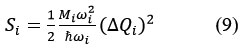
where, ΔQi = (ground and excited states displacement area), Mi = (reduced ionic mass for the i mode). This HR factor is related also to the relaxation energy Erel, That provides information about the intensity of the electron-phonon coupling.

Figure 6(a) shows that the PL peaks are not equidistant, which imply the existence of at least two vibrating oscillators 25. The PL spectra can be modeled according to formula (11).

where, E0 is the 0-0 transition energy and Γ is the Gaussian function with constant width σ.
The PL spectrum of the 5 µm oligomer thin film exhibit two peaks at 400 and 420 nm ascribed to monomer and excimer states of oligomer in thin films respectively. It can be clearly observed from PL spectra of the HOTF pristine oligomer that by increasing thickness the excimer emission becomes dominant. The normalized PL spectra of oligomer and blends are modeled by a sum of FC and Gaussian fits.
 |
Figure 7: Experimental PL spectra (black dashed line) and theoretical spectra (red solid line) (a) 5 µm of Oligomer (b) 12 µm of Oligomer (c) 18 µm of Oligomer thin films; |
 |
Figure 8: Experimental PL spectra (black dashed line) and theoretical spectra (red solid line) (a) Oligomer: ZnO (1 mg) (b) Oligomer: ZnO (1.5 mg) (c) Oligomer: ZnO (2 mg) blends thin films; |
Figure 7 and Figure 8 represent the best fitting of the experimental data related to the normalized PL spectra of the HOTF pristine oligomer for different thicknesses and HOTF: ZnO nanoparticles blends for different concentration of ZnO. The involved modes 0.103, 0.158, 0.174 and 0.198 eV, weredetected by Raman spectroscopy. The strong mode 0.198 eV assigned to ring stretching mode and the other modes attributed to C-C stretching modes between phenylene rings and C-H in-plane bending modes 26,27.
Figure 7 shows the experimental emission spectra (black dashed line) with the theoretical spectra (red solid line), for different thicknesses of oligomer. For the calculation of the PL spectra of the oligomer, we have used a sum of FC fit (blue dashed line) related to the monomer emission and a Gaussian fit (Green solid line) related to the presence of excimer. The relative Gaussian is centered at 2.952 eV for different thickness of the HOTF oligomer. This excimer emission is due to molecular interaction.
For blends thin films as shown in Figure 8, the PL spectra are modeled also by sum of FC and Gaussian fits. Indeed, the addition of ZnO nanoparticles leads to the enhancement of the excimer emission, where the relative Gaussian is centered at 2.952 eV for the different concentrations of ZnO nanoparticles 1, 1.5 and 2 mg. Table 2 and Table 3 provide a summary of the calculated fitting variables.
Table 2: FC examination of the PL spectrum
|
Samples |
FC fitting parameters |
|
||||||||||
|
|
(eV) |
(eV) |
(eV) |
(eV) |
(eV) |
(eV) |
(MeV) |
|||||
|
Oligomer thin film (5 µm) |
3.1470 |
0.33 |
0.27 |
0.16 |
0.119 |
0.198 |
0.174 |
0.158 |
0.103 |
0.0937 |
149.875 |
|
|
Oligomer thin film (12 µm) |
3.1250 |
0.3 |
0.26 |
0.14 |
0.122 |
0.198 |
0.174 |
0.158 |
0.103 |
0.0650 |
139.326 |
|
|
Oligomer as thin film (18 µm) |
2.7800 |
0.07 |
0.06 |
0.126 |
0.125 |
0.198 |
0.174 |
0.158 |
0.103 |
0.0700 |
57.083 |
|
|
Oligomer: ZnO (1 mg) |
2.7800 |
0.07 |
0.06 |
0.152 |
0.147 |
0.198 |
0.174 |
0.158 |
0.103 |
0.0666 |
63.457 |
|
|
Oligomer: ZnO (1.5 mg) |
2.7799 |
0.07 |
0.06 |
0.151 |
0.146 |
0.198 |
0.174 |
0.158 |
0.103 |
0.0666 |
63.196 |
|
|
Oligomer: ZnO (2 mg) |
2.7797 |
0.07 |
0.06 |
0.150 |
0.145 |
0.198 |
0.174 |
0.158 |
0.103 |
0.0666 |
62.935 |
|
Table 3: Fitting parameters for the Gaussian Fit in the PL spectra; the maximum energy Emax, the amplitude Amp and the widths σ of the Gaussian function.
|
Samples |
Gaussian curves parameters |
||
|
Emax (eV) |
Amp |
σ (eV) |
|
|
Oligomer thin film (5 µm) |
2.952 |
0.05 |
0.0791 |
|
Oligomer thin film (12 µm) |
2.952 |
0.49 |
0.1781 |
|
Oligomer thin film (18 µm) |
2.952 |
0.97 |
0.0700 |
|
Oligomer: ZnO (1 mg) |
2.952 |
0.988 |
0.0700 |
|
Oligomer: ZnO (1.5 mg) |
2.952 |
2.989 |
0.0700 |
|
Oligomer: ZnO (2 mg) |
2.952 |
0.99 |
0.0700 |
From the derived parameters in Table 2, the 0-0 transition energy E0 for the oligomer is red shifted by increasing thickness from 5 to 18 µm. This red shift is related to the increase of the effective conjugation length. This result is in good agreement with the decrease of the relaxation energy Erel by increasing thickness, where Erel decreases with increased oligomer conjugation length 28. From Table 3, the emission of the excimer becomes more important by increasing thickness where the amplitude of Gaussian Fit related to excimer emission increased from 0.05 to 0.97 eV for 5 to 18 µm of the oligomer layer, respectively. Furthermore, the 0-0 transition energy for the oligomer: ZnO blends are slightly red shifted with increasing the concentration of ZnO. This red shift is related to the increase of the conjugation length of the blend by adding ZnO nanoparticles. From our results, and decrease with increasing the amount of ZnO nanoparticles. Thus, ZnO nanoparticles enhanced the conjugation of the HOTF oligomer and leads to the ordered conformation. The blend for 2 mg of ZnO is better ordered than the two other blends. Increasing the amount of ZnO enhances the excimer emission and it is proved by the Gaussian Fit where the amplitude of Gaussian related to excimer emission is about 0.99 eV for 2 mg of ZnO blend.
Conclusion
In conclusion, current-voltage characteristics of light emitting devices based on ZnO nanoparticle with the HOTF oligomer blends have been studied. Characteristic electro-optics parameters hybrid oligomer and ZnO nanopowder have been established. The interfacial charge transfer excitons play a curial role in decreasing the ideality factor by increasing the amount of ZnO nanoparticles. In addition, by the dissociation of CT excitons, the performance of the fabricated LEDs is enhanced with such increment of ZnO nanoparticles. From the Franck-Condon analysis of the PL spectra, the relaxation energy Erel of the pure oligomer thin film decreases with increasing thickness from 5 to 18 µm indicating the increase of the effective conjugation length. The transition energy E0 values for the Oligomer: ZnO blends are slightly red shifted with increasing the concentration of ZnO. This red shift is due to the increase of the conjugation length of the blend by adding ZnO nanoparticles. In addition, it was found that the Huang-Rhys factor decreases by increasing ZnO amount in the blend. Addition of this metal oxide leads to the ordered conformation. Also, the conjugation of the HOTF oligomer is enhanced with adding ZnO nanoparticles. Emission of the excimer is proved by Gaussian Fit where its amplitude is increased by increasing the thickness of the pristine oligomer and by adding ZnO nanoparticles in the blend thin films.
Acknowledgment
The authors would like to thank Imam Mohammad Ibn Saud Islamic University for the financial support of this project under contract number (19-12-12-11).
Conflict of Interest
The authors declare that there is no conflict of interest regarding the publication of this paper.
References
- Gledhill SE, Scott B, Gregg BA. J Mater Res. 2005 .20(12):3167-79.
CrossRef - Liang FX, Gao Y, Xie C, Tong XW, Li ZJ, Luo LB. J MaterChem C.2018;6(15):3815-33..
CrossRef - Singh P, Kumar R, Singh RK. Ind. Eng. Chem. Res. 2019,19;58(37):17130-63.
CrossRef - Wang YP, Li HC, Huang YC, Tan CS. Inorganics. 2023 Jan 11;11(1):39.
CrossRef - Franco MA, Conti PP, Andre RS, Correa DS. Sensors and Actuators Reports. 2022 , Sens. Actuators Rep .10:100100.
CrossRef - Han WB, Yang SM, Rajaram K, Hwang SW. Adv. Sustainable Syst. 2022 ;6(2):2100075.
CrossRef - Yang Y, Duan S, Zhao H. Nanoscale. 2022;14(32):11484-511.
CrossRef - Bishnoi S, Datt R, Arya S, Gupta S, Gupta R, Tsoi WC, Sharma SN, Patole SP, Gupta V. Adv. Mater. Interfaces. 2022 ;9(19):2101693.
CrossRef - Ul Hasan K, Sandberg MO, Nur O, Willander M. Adv. Opt. Mater. 2014;2(4):326-30.
CrossRef - Krupin AS, Karyakin ME, Knyazev AA, Galyametdinov YG. AIP Conference Proceedings. 2022 Jun 10 (Vol. 2466, No. 1, p. 060036). AIP Publishing LLC.
- Mustapha N, Rafea MA, Aldaghri O, Abdelaziz BB, Ibnaouf KH. J. Mater. Sci.: Mater. Electron. 2021 ;32:5473-81.
CrossRef - Hernandez-Como N, Rivas-Montes G, Hernandez-Cuevas FJ, Mejia I, Molinar-Solis JE, Aleman M. Mater. Sci. Semicond. Process. 2015 , 1;37:14-8.
CrossRef - Cheung SK, Cheung NW. Appl. Phys. Lett. 1986, 14;49(2):85-7.
CrossRef - Güllü Ö, Türüt A. Mater. Sci.-Pol. 2015 , 1;33(3):593-600.
CrossRef - Tripathi SK, Sharma M. J. Appl. Phys. 2012 ,1;111(7):074513.
CrossRef - Mridha S, Basak DJ. Appl. Phys. Lett. 2008 .7;92(14):142111.
CrossRef - Lapa HE, Kökce A, Aldemir DA, Özdemir AF, Altındal Ş. Indian J. Phys.. 2020 ;94:1901-8.
CrossRef - Ikenoue T, Kameyama N, Fujita S. Phys. Status Solidi C. 2011 ;8(2):613-5.
CrossRef - Hernandez-Como N, Rivas-Montes G, Hernandez-Cuevas FJ, Mejia I, Molinar-Solis JE, Aleman M. Mater. Sci. Semicond. Process. 2015 , 1;37:14-8.
CrossRef - Wu W, Bian JM, Sun JC, Cheng CH, Wang YX, Luo YM. J. Alloys Compd. 2012 Sep 5;534:1-5.
CrossRef - Scharsich C, Fischer FS, Wilma K, Hildner R, Ludwigs S, Köhler A. J. Polym. Sci., Part B: Polym. Phys. 2015 Oct 15;53(20):1416-30.
CrossRef - Clark J, Silva C, Friend RH, Spano FC. Phys. Rev. Lett. . 2007 May 17;98(20):206406.
CrossRef - Hagler TW, Pakbaz K, Voss KF, Heeger AJ. Phys. Rev. B. 1991 Oct 15;44(16):8652.
CrossRef - Spano FC, Silva C. Annu. Rev. Phys. Chem.. 2014 Apr 1;65:477-500.
CrossRef - Khan AL, Sreearunothai P, Herz LM, Banach MJ, Köhler A. Phys. Rev. B. 2004 Feb 4;69(8):085201.
CrossRef - Ariu M, Sims M, Rahn MD, Hill J, Fox AM, Lidzey DG, Oda M, Cabanillas-Gonzalez J, Bradley DD. Phys. Rev. B. 2003 May 30;67(19):195333.
CrossRef - Brown PJ, Thomas DS, Köhler A, Wilson JS, Kim JS, Ramsdale CM, Sirringhaus H, Friend RH. Phys. Rev. B. 2003 Feb 28;67(6):064203.
CrossRef - Lin Y-Y. Chen C-W, J. Chang, Lin T.Y., I.S. Liu, Su W-F.. Nanotechnology. 2006 17 (5) 1260-1263.
CrossRef - S.P. Kennedy, N. Garro, R.T. Phillips . Phys. Rev. B. 2001. 64 (11) 115206.
CrossRef

This work is licensed under a Creative Commons Attribution 4.0 International License.
About The Author
![]()
A New Edition of Web of Science
Journal Impact Factor
2022: 0.5
Five Year: 0.8
Journal is Indexed in

Cabells Whitelist
![]()


