Effect of pH on the Synthesis of Cobalt Selenide Films by SILAR Method
Ho Soon Min1* and Ng Sha Shiong2
1INTI International University Putra Nilai, Negeri Sembilan, Malaysia.
2Institute of Nano Optoelectronics Research and Technology, Universiti Sains Malaysia, 11800 USM, Penang, Malaysia
Corresponding Author E-mail: soonmin.ho@newinti.edu.my
DOI : http://dx.doi.org/10.13005/ojc/370404
Article Received on : 30-Apr-2021
Article Accepted on : 02-Jul-2021
Article Published : 09 Jul 2021
Reviewed by: Dr. A. Cyril
Second Review by: Dr. Surya Hadi
Final Approval by: Dr. M.A Shah
The successive ionic layer adsorption and reaction method or called SILAR method was used to produce cobalt selenide thin films for the first time. The deposition was carried out onto the substrate under different various pH values. The X-ray diffraction (XRD), field emission scanning electron microscope (FESEM) and ultraviolet visible spectrophotometer were used to investigate the structure, morphology and optical properties of thin films, respectively. The XRD patterns confirmed that the presence of cubic phase cobalt selenide thin films. The grain size increased with increasing the pH value from pH 2 to pH 4 based on the FESEM images. The band gap values are in the range of 2 eV to 2.5 eV.
KEYWORDS:Band Gap; Cobalt Selenide; Semiconductor; SILAR Method; Thin Films
Download this article as:| Copy the following to cite this article: Soonmin H, Shiong N. S. Effect of pH on the Synthesis of Cobalt Selenide Films by SILAR Method. Orient J Chem 2021;37(4). |
| Copy the following to cite this URL: Soonmin H, Shiong N. S. Effect of pH on the Synthesis of Cobalt Selenide Films by SILAR Method. Orient J Chem 2021;37(4). Available from: https://bit.ly/3dZd9q0 |
Introduction
The metal sulfide 1-3, metal selenide 4-6 and metal telluride films 7-9 have attracted great attention because of cost effective materials and low toxicity. The obtained films could be used in the solar control device, holographic, laser device 10, sensor devices 11, solar cell 12-15 and other optoelectronic devices 16. The metal chalcogenide thin films have been produced by using different deposition techniques 17-22 such as electro deposition, spray pyrolysis, radio frequency sputtering, chemical vapour deposition, thermal evaporation, chemical bath deposition, solvo-thermal method, and successive ionic layer adsorption and reaction (SILAR) method.
SILAR method is one of the solution phase methods for depositing thin films on a variety of substrates 23. In this deposition method, the substrate is immersed in turn into the solution (containing cation and the anion precursor) 24. During the experiment, the substrate is rinsed with distilled water, between the cation and anion immersions. The thin film growth takes place through the adsorption and reaction of these ions. By repeating these cycles, the thin films are produced successfully onto substrate 25.
Over the past few decades, the SILAR method has attracted considerable attention because of its high potential for deposition of thin films with thickness ranging from tenths of nanometers to several micrometers 26. The unique features offered by the SILAR method are: (i) to grow the undoped doped thin films, (ii) suitable for mass production, (iii) it does not require vacuum systems because the deposition can be conducted under atmospheric conditions; hence it is relatively simple and inexpensive as compared to physical vapour deposition (PVD) methods, (iv) the deposition process is carried out at low temperature (typically at room temperature), hence temperature sensitive substrates (such as polymer) can be used, (v) the starting materials used are commonly available and relatively cheap, hence, a variety of materials can be produced, (vi) the deposition is conducted by alternating immersion of the substrate in solutions containing the cation and anion ions, respectively 27, rinsing of the substrate with distilled water, hence all the precursor solutions are recyclable, (vii) the film thickness could be controlled using deposition cycles 28.
Nevertheless, the SILAR method possesses several disadvantages 29 as compared to other deposition techniques. These include (i) slow deposition rate and the deposition cycle about 1 – 3 Å. (ii) the deposited films have fairly high oxygen contamination (iii) not all substrates are suitable to be used due to instability of material (iv) hard to deposit ternary or quaternary alloys due to the difference in solubility products.
The main objective of this experiment is to study the influence of pH on the properties of cobalt selenide thin films deposited onto a microscope glass substrate. This is the first time we report the characterization of SILAR deposited films by using different tools such as XRD, FESEM and ultraviolet-visible spectrophotometer.
Experimental
Preparation of thin films
Cobalt (II) chloride hexahydrate (CoCl2.6H2O) and sodium selenite (Na2O3Se) were used without further purification. A microscope glass slide was used as a substrate during the deposition process. This substrate was cleaned by acetone, and de-ionized water before use. During the deposition process, the glass substrate immersed in the 0.2 M cationic solution (Co2+ ion) for 30 seconds. After rinsing with de-ionized water for 10 seconds, it was immersed in 0.2 M anionic solution (Se2- ions) for 30 seconds. Then, rinsing with de-ionized water for 10 seconds again in order to remove the loose material on it. The reaction solutions were put in a beaker under various pH values (pH 2 and pH 4). The sodium hydroxide (NaOH) and hydrochloric acid (HCl) were used to adjust pH value. After the deposition process (after 12 cycles), the films were collected, rinsed by de-ionized water, and finally, put in the oven for 24 hours.
Characterization of thin films
The X-ray diffraction analysis was carried out to study the structure properties of the films. This technique was done by using a Malvern Panalytical diffractometer for the 2q ranging from 10° to 80° with CuKα (λ = 0.15418 nm) radiation. The field emission scanning electron microscope (FEI, Nova Nanosem 230) was employed to investigate the surface morphology of the films. UV-visible spectrophotometer (Perkin Elmer UV/Vis Lambda 35) was utilized to study the optical properties of films. The thin films were placed across the sample radiation pathway while the cleaned microscope glass slide was put across the reference path. The band gap energy of the films was calculated based on the absorption data.
Results and discussion
Binary, ternary, quaternary and penternary metal chalcogenide thin films have been prepared by using various deposition techniques such as the physical and chemical deposition techniques 30-32. Researchers have concluded that the selection of deposition method depends on production cost, specific application, the properties of films and available resources. Researchers have reported that these materials have a great impact on the modern era of technology. The obtained nanostructured films could be used in the different fields such as solar cells, optical switching devices, energy storage devices, environmental applications, laser devices, photo catalysts, optical sensors and telecommunications devices. Abundant literature is available on the preparation of cobalt sulphide 33-38, cobalt telluride 39-42 and cobalt selenide 43-48 thin films via various deposition techniques. In this work, SILAR method was selected to produce cobalt selenide films due this deposition technique has many advantages if compared to other deposition techniques. We report for the first time the synthesis of cobalt selenide using cobalt (II) chloride hexahydrate and sodium selenite solution.
 |
Figure 1: FESEM images for the cobalt selenide films prepared at [a] pH 2 [b] pH 4. |
The field emission scanning electron microscope (FESEM) was used to characterize the morphology of prepared films. The figure 1 showed the FESEM images of SILAR deposited cobalt selenide thin films under different pH values. The average grain sizes were about 0.2- 4 µm and 5 µm for the films prepared at pH 2 and pH 4, respectively. A slight increase of the grain size follows the pH increasing could be observed. Concerning the nucleation stage film growth proceeds by nucleation of crystallites, then forming grains which coalesce to cover the substrate surface and to show a dense structure. These results are consistent with several other studies 49-51.
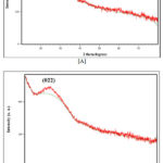 |
Figure 2: XRD patterns for the cobalt selenide films prepared at [a] pH 2 [b] pH 4. |
Figure 2 indicated the X-ray diffraction (XRD) patterns for the cobalt selenide thin films produced under different pH values. Based on the figure, the XRD patterns showed diffraction peak at 2q=24°, which can be indexed as reflection from the (022) plane of the cubic structure Co9Se8 compound. Other scientists have highlighted similar findings (cubic cobalt selenide structure) in the literature 52, 53. The obtained X-ray diffraction patterns were well matched with the standard Joint Committee on Powder Diffraction Standards (JCPDS) (Reference code: 98-004-4857). Based on the JCPDS data, lattice parameter values are a=b=c=10.431 Å. The crystal system, space group and space group number were cubic, Fm-3m and 225, respectively.

Figure 3 showed the UV-visible absorption spectra in the wavelength regions of 300 to 1000 nm. Generally, we see that all the samples indicated high absorption in the visible range, which make these materials possible to use in the photo electrochemical cell and solar cells. Then, the absorbance decreases with the increasing of wavelength. A similar tendency was also found by other researchers 54, 55. From the figure, we noted that the highest absorbance value could be seen for the films produced at pH 4. Due to increasing in the grain size with thickness. Bigger size reduces the reflectivity of incident photon on the surface of films as reported 49, 50. The band gap was calculated based on the Stern equation. This is a very useful method and has been reported by many scientists 56-62.
where v is the frequency, h is the Planck’s constant, k equals a constant while n carries the value of either 1 or 4. The n value is 1 for a direct gap material and 4 for indirect gap material. The plot of (Ahν)2 against hν is indicated in figure 4. Extrapolation of the linear portion of the curve to (Ahν)2=0 produce the band gap energy. The band gap increased from 2 eV (pH 4) to 2.5 eV (pH 2) as shown in figure 4. Other scientist groups have highlighted similar band gap values in the literature (Table 1). These cobalt selenide films have been prepared by using different methods including chemical bath deposition, electro deposition, magnetron sputtering method and mechano chemical method. The obtained thin films could be used in solar cell applications because of direct band gap between 1 to 2 eV 63, 64.
 |
Figure 3: Optical absorbance spectra of cobalt selenide films prepared at [a] pH 2 [b] pH 4. |
 |
Figure 4: Plots of (Ahv)2 versus (hv) for cobalt selenide thin films prepared at different pH values [a] pH 2 [b] pH 4. |
Table 1: Band gap energy of cobalt selenide thin films prepared under different deposition techniques.
|
Remarks |
Band gap (eV) |
Reference |
|
Ammonia, cobalt (II) acetate and sodium selenosulphite were used to prepare thin films onto glass slide via chemical bath deposition technique |
1.8 to 3.6 |
Ghobadi and co-workers, 2019 [43] |
|
Electro deposition method was used to prepare thin films onto tin oxide glass substrate in the presence of H2SeO3 and Co(CH3COO)2 solutions. |
1.53 |
Liu and co-workers, 2010 [44] |
|
Chemical bath deposition method was used to prepare thin films onto non-conducting micro glass slide. The chemical bath contained cobalt nitrate, ammonia and sodium selenosulphate. |
1.7 |
Muddsar and co-workers, 2014 [45] |
|
Magnetron sputtering method was used to synthesize thin films onto substrate. |
1.53 |
Zhu and co-workers, 2006 [46] |
|
Electro deposition technique was used to prepare thin films onto substrate (tin oxide coated glass). |
1.53 |
Wang and co-workers, 2011 [47] |
|
Thin films were grown using the mechanochemical method. |
1.7 |
Nina and co-workers, 2017 [48] |
Conclusion:
The cobalt selenide thin films have been successfully deposited onto glass substrate using SILAR deposition technique. This deposition method is attracting due to inexpensive, simple and convenient for low temperature deposition process. The films prepared at pH 4 showed the highest absorbance value, biggest size and band gap of 2 eV.
Acknowledgement
This research project was sponsored by INTI International University (INTI Internal Research Grant INTI –CAE-01-01-2018).
Conflicts of Interest
Authors declared that there is no conflict of interest.
References
- Yesica, B.; Luis, A. Mater. Sci. Semicond. Process., 2021, 121, https://doi.org/10.1016/j.mssp.2020.105405.
CrossRef - Anuar, K.; Ho, S.M.; Saravanan, N.; Abdul, H.; Noraini, K. Dig. J. Nanomater. Biostructures, 2010, 5, 975-980.
- Emegha, J.; Damisa, J.; Elete, D.; Arijaje, T.; Ogunile, P. J. Phys. Conf. Ser., 2021, https://doi.org/10.1088/1742-6596/1734/1/012045.
CrossRef - Li, X.; Wang, S.; Liao, H.; Yang, S.; Liu, X. Opt. Mater., 2021, 111, https://doi.org/10.1016/j.optmat.2020.110698.
CrossRef - Ho, S.M. Am. Chem. Sci. J., 2016, 14, 1-6.
- Gaur, M.; Bhuse, V.; Sanadi, R. Optik, 2021, 227, https://doi.org/ 10.1016/j.ijleo.2020.166057.
CrossRef - Li, C.; Wang, Y.; Ren, S.; Wang, W. Mater. Sci. Semicond. Process, 2021, 121, https://doi.org/10.1016/j.mssp.2020.105341.
CrossRef - Ho, S.M.; Sharma, D.; Olusola, O. Asian J. Chem., 2018, 30, 469-473.
CrossRef - Dhasade, S.; Han, S.; Fulari, J. J. Semicond., 2012, 33, https://doi.org/10.1088/1674-4926/33/9/093002.
CrossRef - Chao, J.; Li, M.; Zhang, S.; Liu, T. Mater. Res. Bull., 2018, 107, 54-59.
CrossRef - Syed, T.; Abu, B.; Bibi, S.; Muhammad, B. Appl. Surf. Sci., 2012, 258, 9610-9616.
CrossRef - Tizazu, A; Hone, F. Int. J. Thin Films Sci. Technol., 2019, 8, 43-53.
- Chate, P.; Sathe, D.; Sankpal, U. Int. J. Thin Films Sci. Technol., 2020, 9, 31-35.
- Ho, S.M. Makara J. Sci., 2017, 21, 119-124.
- Ranojit, D. Int. J. Thin Films Sci. Technol.,2020, 9, 21-25.
CrossRef - Santhosh, T.; Kasturi, V.; Shivakumar, G. Mater. Today Proc.,2016, 3, 2220-2224.
CrossRef - Babu, D.; Shajan, S.; George, A.; Kumaresan, S. Mater. Sci. Semicond. Process, 2017, 63, 127-136.
CrossRef - Cui, Y.; Shao, H.; Zhang, Z.; Wang, Z.; Li, J. J. Nanosci. Nanotechnol., 2020, doi: 10.1166/jnn.2020.17209.
CrossRef - Daniel, T.; Nishanthi, S.T.; Mphanraj. K.; Sivakumar, G. Vacuum, 2019, 161, 138-142.
CrossRef - Anuar, K.; Saravanan, N.; Zulkefly, K.; Atan, S.; Tan, W.T.; Ho, S.M. Bull. Chem. Soc. Ethiop.,2010, 24, 259-266.
- Hao, G.; Shen, H.; Gao, C.; He, X. J. Mater. Sci. Mater. Electron, 2013, 24, 3195-3198.
CrossRef - Anuar, K.; Saravanan, N.; Tan, W.T.; Ho, S.M.; Teo, D. Leonardo J. Sci.2010, 16, 1-12.
- Çayır, T. Vacuum, 2019, 167, 189-194.
CrossRef - Akaltun, Y.; Aslan, M.; Yetim, T.; Çayır, T. Surf. Coat. Technol., 2016, 292, 121-131.
CrossRef - Lindroos, S.; Leskela, M. “Successive Ionic layer adsorption and reaction (SILAR) and related sequential solution – Phase deposition techniques,” in Solution Processing of Inorganic Materials, D. B. Mitzi, Ed. Hoboken, New Jersey, USA: John Wiley & Sons, Inc., 2009, pp. 239 – 287.
CrossRef - Pathan, H.; Lokhande C. Bull. Mater. Sci., 2004, 27, 85–111.
CrossRef - Sundhar, A. Mater. Today Proc., 2020, https://doi.org/ 10.1016/j.matpr. 2020.09.550 (2020).
CrossRef - Anbazhagan, M.; Siva, V.; Abdul, S.; Sultan, B. J. Alloys Compd., 2021, 856, https://doi.org/10.1016/j.jallcom.2020.158055.
CrossRef - Pawan, K.; Rao, G.; Ashik, D. ECS J. Solid State Sci. Technol., 2020, https://doi.org/10.1149/2162-8777/aba0cd.
CrossRef - Nadareishvili, M.; Mamniashvili, G.; Jishiashvili, D.; Ramana, C.; Ramsden, J. Eng. Technol. Appl. Sci. Res., 2000, 10, 5524-5527.
CrossRef - Ben, T.; Mahboub, D.; Jemai, M.; Belgacem, S. Eng. Technol. Appl. Sci. Res., 2019, 9, 4695-4701.
CrossRef - Ho, S.M. Eng. Technol. Appl. Sci. Res., 2000,10, 6161-6164.
CrossRef - Sartale, S.; Lokhande, C. Indian J. Pure Appl. Phys., 2000, 38, 48-52.
- Abza, T.; Dadi, D.; Hone, F.; Chebelew, T.; Ahmed, K. Adv. Mater. Sci. Eng., https://doi.org/10.1155/2020/2628706.
CrossRef - Mane, S.; Kamble, S.; Deshmukh, P. Mater. Lett., 2011, 65, 2639-2641.
CrossRef - Geetha, G.; Priya, M.; Suresh, S. Mater. Res., 2017, 20, 62-67.
- Kale, B.; Abhishek, L.; Rahul, B.; Lokhande, D. J. Colloid Interface Sci., 2018, 532, 491-499.
CrossRef - Karthik, R.; Malik, M.; Raftery, J.; Tuna, F.; Paul, O. Chem. Mater., 2010, 22, 4919-4930.
CrossRef - Jee, H.; Paeng, K.; Son, Y.; Jang, Y.; Rho, K. J. Electrochem. Soc., 2019, 166, https://doi.org/10.1149/2.0101905jes.
CrossRef - Dahal, B.; Dulal, P.; Pegg, L.; Philip. J. Vac. Sci. Technol. B, 2016, 34, https://doi.org/10.1116/1.4959576.
CrossRef - Zhang, G.; Liu, K.; Zhou, J. J. Mater. Chem. A, 2018, 6, 6335-6343.
CrossRef - Tanori, O.; Mendiola, E.; Gamez, R.; Ibarra, A. Chalcogenide Lett., 2019, 16, 57-61.
- Ghobadi, N.; Hafezi, F.; Naderi, S.; Habibi, M.; Mardani, M. Semicond., 2019, 53, 1751-1758.
CrossRef - Liu, F.; Wang, B.; Lai, Y.; Zhang, Z.; Liu, Y. J. Electrochem. Soc.,2010, https://doi.org/10.1149/1.3468675.
CrossRef - Muddsar, G.; Hankare, P.; Kalyanrao, G.; Imtiaz, M.; Bhuse, V. New J. Chem., 2014,DOI: 10.1039/C3NJ00924F.
CrossRef - Zhu, L.; Lam, A.; Susac, D.; Teo, M.; Parsons, R. J. Solid State Chem., 2006, 179, 3942-3948.
CrossRef - Wang, B.; Liu, Y.; Jie, L.; Lai, Y.; Zhang, Z. J. Inorg. Mater., 2011, DOI: 10.3724/SP.J.1077.2011.00403.
CrossRef - Nina, D.; Anna, Z.; Marcela, A. Appl. Phys. A, 2017, https://doi.org/ 10.1007/s00339-017-0785-9.
CrossRef - Nasr, T.; Kamoun, N.; Kanzari, M.; Bennaceur, R. Thin Solid films, 2006, 500, 4-8.
CrossRef - Gitashri, A.; Saikia, P.; Bora, J. Mater. Chem. Phys., 2020, https://doi.org/10.1016/j.matchemphys.2019.122277.
CrossRef - Higareda, A.; Mis, R.; Rimmaudo, I.; Pena. L. Superlattices Microstruct., 2021, https://doi.org/10.1016/j.spmi.2021.106831.
CrossRef - Gaur, M.; Hankare, P.; Mulla, S.; Bhuse, M. J. Mater. Sci. Mater. Electron., 2016, 27, 7603-7608.
CrossRef - Panneerselvam, A.; Nguyen, C.; Waters, J.; Malik, A.; Paul, O. Dalton Trans., 2008, https://doi.org/10.1039/B802012D.
CrossRef - Pathan, K.; Siddiquee, H.; Alam, S.; Islam, O.; Gafur, M. J. Mater. Sci. Mater. Electron., 2013, 24, 745-751.
CrossRef - Khalaf, M.; Baha, M.; Ausama, I.; Anwar, A. Photonics Nanostructures Fundam. Appl., 2016, 18, 59-66.
CrossRef - Teo, S.; Zainal, Z.; Tan, T.; Imad, H. Malaysian J. Anal. Sci.,2008, 12, 600-608.
- Sachin, H.; Patil, K.; Lad, S.; Bhagwat, M. Arch. Phys. Res. 2013, 4, 7-11.
- Jigi, G.; Abza, T.; Girma, A. J. Appl. Biotechnol. Bioeng., 2021, 8, 55-58.
- Kumarage, C.; Wijesundera, P.; Kaur, N.; Zappa, D.; Jayalath, C.; Dassanayake, S. Inter. J. Electroactive Mater., 2019, 7, 1-6.
- Kassim, A.; Ho, S.M.; Abdul, H.; Tan, W.T.; Saravanan, N. Macedonian J. Chem. Chem. Eng., 2010, 29, 97-103.
CrossRef - Anuar, K.; Ho, S.M.; Yazid, M. Inter. J. Chem. Res., 2011, 3, 21-26.
- Saravanan, N.; Ho, S.M.; Kassim, A.; Tan, W.; Teo, D. Leonardo J. Sci., 2010, 16, 1-12.
- Ho, S.M. Inter. J. Chem. Sci., 2016, 14, 143-151.
- Sinha, T.; Verma, L.; Ayush, K. Appl. Phys., 2020, https://doi.org/ 10.1007/s00339-020-04058-4.
CrossRef

This work is licensed under a Creative Commons Attribution 4.0 International License.
About The Author
![]()
A New Edition of Web of Science
Journal Impact Factor
2022: 0.5
Five Year: 0.8
Journal is Indexed in

Cabells Whitelist
![]()


