Preparation of N-TiO2/PbS Nanocomposite Using Successive Ionic Layer Adsorption and Reaction (SILAR) Method
Anti Kolonial Prodjosantoso , Nikmahtul Eviana, Cahyorini Kusumawardani and Kristian Handoyo Sugiyarto
Department of Chemistry, Yogyakarta State University, Yogyakarta, 55281, Indonesia.
Corresponding Author E-mail: prodjosantoso@uny.ac.id
DOI : http://dx.doi.org/10.13005/ojc/340523
Article Received on : 29-08-2018
Article Accepted on : 05-09-2018
Article Published : 13 Oct 2018
Titanium oxides are wellknown semiconductor and have been studied intensively in term of their physical and chemical properties, and also the applications. The oxides have been modified in many ways to improve the catalitic capability. Nitrogen has been doped and dyes have been introduced into TiO2. N-TiO2/PbS nanocomposite has been synthesized using successive ionic layer adsorption and reaction (SILAR) method, by which ITO glass layered with N-TiO2 was immersed several cycles in a homogenous mixture of Pb(CH3COO)2 and (NH4)2 S. The combination method of XRD, UV-Vis, and SEM have been used to characterize the samples. It is confirmed that N-TiO2/PbS exists in the samples. The particle size of PbS is about 6-8 nm. The UV-Vis study reveals that the Eg1 of N-TiO2/PbS is lower than that of Eg of N-TiO2 itself, and the Eg2 ie. about 1.62 eV.
KEYWORDS:Nanocomposite; Pbs; SILAR; Solar Cell
Download this article as:| Copy the following to cite this article: Prodjosantoso A. K, Eviana N, Kusumawardani C, Sugiyarto K. H. Preparation of N-TiO2/Pbs Nanocomposite Using Successive Ionic Layer Adsorption and Reaction (SILAR) Method. Orient J Chem 2018;34(5). |
| Copy the following to cite this URL: Prodjosantoso A. K, Eviana N, Kusumawardani C, Sugiyarto K. H. Preparation of N-TiO2/Pbs Nanocomposite Using Successive Ionic Layer Adsorption and Reaction (SILAR) Method. Orient J Chem 2018;34(5). Available from: http://www.orientjchem.org/?p=50703 |
Introduction
Solar energy, a clean, non-polluting, safe, and unlimited energy, has been proposed to alternatively replace the nonrenewable energy sources, such as coal and oil.1 The availability of solar energy in the form of sunlight received by the earth’s surface is much more than enough to cover the energy consumed by the entirely world today.2 However, we need an efficient photovoltaic technology using semiconductor devices called solar cells for converting the sunlight directly into electrical energy.3
In the last few decades, for example, the titanium oxide (TiO2) has been enormously studied. Although TiO2 is very promising, there are still shortcomings. The pure TiO2 can only be activated under UV light irradiation (hυ<390 nm) because of its large band gap energy (3-3.4 eV). In order to extend the light absorption edge to visible region, many attempts have been undertaken.4 A combination of organic-inorganic nanostructure semiconductor has been attempted to prepare superior solar cells.5,6 The dye-sensitized solar cell (DSSC) based on titanium dioxide (TiO2) having an efficiency of 11% has also been applied for the solar cell.7 Asahi et al. succeeded in increasing the visible light absorption properties of TiO2 semiconductors through nitrogen deposition.8 The addition of N to the TiO2 frame work results in a band gap narrowing caused by the overlapping of the N 2p with the O 2p orbitals. Furthermore, the use of N-TiO2 materials can improve the efficiency and stability of solar cells.9,10 However, the more stable compounds such as CdS, CdSe, PbS, and In As have been proposed to prepare semiconductors.11 In this study, PbS was introduced to the N-TiO2 material by successive ionic layer adsorption reaction (SILAR) method, to prepare N-TiO2/PbS nanocomposite.
Materials and Methods
Materials. Titanium tetraisopropoxide (TTIP) (Merck 97%), ethylenediamine (Merck ≥99%), (NH4)2S (Merck ≥ 20%), Triton-X (Merck), Pb(CH3COO)2.3H2O (Merck ≥99,5%), acetyl acetic acid (Merck 100%), and ITO glass substrates (Dyesol) have been used as received without any prior treatments.
Methods. X-ray powder diffraction (XRD) analysis was carried out using XRD Rigaku Miniflex 600 with Cu Kα radiation (λ=1.5405981 Å), operated at 40 kV and 30 mA. Scanning electron microscopy (SEM) measurement was performed on SEM JEOL JED-2300. UV–vis diffuse reflectance spectra (DRS) were determined by a UV-Vis UV 1700 Pharmaspec Spectrophotometer Specular Reflectance Attachment.
Synthesis of N-TiO2 NPs
The N-TiO2 NPs was synthesized using the method developed by Zhou et al.12 A quantity of 6.7 mL ethylenediamine was dissolved in 80 mL of absolute ethanol and stirred for 2 hours to obtain homogeneous solution. 3 mL TTIP was added dropwise into the solution while stirring for 1 hour. The resulted homogeneous solution was refluxed at 80°C for 6 hours, and then cooled to room temperature, and added with 15 mL glacial acetic acid. Hydrolysis was carried out with the addition of 21.6 mL of demineralized water dropwise followed by stirring for 24 hours. The smixture was allowed to stand for 24 hours and the yellow solids obtained was filtered off. The solidwas dried at 80°C for 8 hours, and calcined at 450°C for 4 hours with heating rate of 2°C per minute to produce the N-TiO2 NPs powder.
The N-TiO2 thin layer was prepared on ITO glass substrates of 2.5 x 1.5 cm2. A 2 g of N-TiO2 powder was thoroughly mixed with 0.05 mL of triton-X and 0.01 mL acetyl acetone to produce a paste which was then deposited onto the glass substrate surface by the doctor blade technique,13 and calcined at 400oC for 2 hours.
Preparation of N-TiO2/PbS was carried out by applying Pb2+ and S2- ions on the N-TiO2 substrate. The N-TiO2 substrate was preheated using an oven at 60°C for 10 minutes, and immersed varies between 1, 5, 15, 25, and 50 cycles for 10 seconds each into a mixture of 0.2 M of Pb(CH3COO)2 and 0.4 M of (NH4)2S solutions, and finally air dried.
Results and Discussion
N-TiO2/PbS nanocomposite has been prepared using a successive ionic layer adsorption and reaction (SILAR) method with 1, 5, 15, 25, and 50 cycle’s variation. The powder XRD patterns of N-TiO2/PbS nanocomposites, ITO, PbS and N-TiO2 materials can be seen in Figure 1. In general, the XRD patterns of N-TiO2/PbS nanocomposites indicate the presence of TiO2 (anatase), ITO and PbS phases. The line at 2q about 26.20o indicates the TiO2 (anatase) (Figure 1.b to 1.g), performing that the character of TiO2 still remains after the immersion processes. The surface of N-TiO2 layered by PbS could be recognized by the presence of selected but characteristic diffractogram of PbS at 2q about 30.15o (Figure 1.b to 1.h). The stronger peak relates to the more immersion the N-TiO2 into the Pb2+ and S2- solution, and so the more PbS adsorbed onto the surface of N-TiO2. Despite the strong intensity may be resulted by the high crystallinity of PbS. A selected peak in the red-dashed box (Figure 1.b) indicates the absence of PbS from unimmersed sample. Some strong peaks of ITO are also observed at 2q about 27.23oC, 34.42o, and 38.48oC, and 52.23oC.
The XRD of PbS consists of planes (111), (200), (220), (311), and (222).14,15 The XRD spectra of N-TiO2/PbS one cycle shows no peaks of PbS, but only TiO2 and ITO. This is propably occured as only very little amount of PbS is adsorbed on the surface of N-TiO2. The PbS spectra are observed at XRD pattern of N-TiO2 5 cycle. However, the spectra are weak and are not clearly visible. This may be due to improper crystal orientation, so that when the crystal is subjected to X-rays, many of the diffracted rays out of the detector. Observable PbS spectra are seen in the N-TiO2/PbS spectra of 15, 25, and 50 cycles (Figure 1.e-1.g).
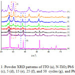 |
Figure 1: Powder XRD patterns of ITO (a), N-TiO2/PbS with 0 (b), 1 (c), 5 (d), 15 (e), 25 (f), and 50 cycles (g), and PbS (h). |
The size of PbS crystallite over the N-TiO2 can be determined from the broadening of corresponding X-ray spectral peak by Scherrer formula:16
![]()
where D is crystallite size (nm), k is a material constant (0.9), λ is the X-ray wavelength used for the measurement (nm), β is the selected peak FWHM. The PbS crystallite sizes are listed in Table 1. The crystallite size of PbS material is ranged from 6.05 nm to 8.07 nm (Table 1). This is in agreement with Popa et al. stating that the size of PbS crystallite is between 5 to 20 nm.17
Tabel 1: Crystallite size of PbS over the N-TiO2.
| Cycle variation (time) | Crystallite size (nm) |
| 5 | 7.51 |
| 15 | 7.84 |
| 25 | 8.07 |
| 50 | 6.05 |
The UV–vis diffuse reflectance spectra of the N-TiO2/PbS samples are shown in Figure 2. Obviously, the UV–vis adsorption edge of N-TiO2/PbS shifts to the visible-light region along with the more immersion cycles. The absorbance of the PbS-sensitized N-TiO2 samples is not proportional to the number of immersion cycles, although at the time of immersion the formation of black color of the PbS was getting darker along with the number of immersions. The resulting absorbance value is depend on the non-uniform particle size of N-TiO2/PbS absorbing light with different energy.
Furthermore, N-TiO2/PbS samples indicate two characteristic light absorption edges. The first absorption edge corresponds to the electron promotion from the valence to the conduction bands, while the other originates from the new energy levels in the forbidden band of TiO2 formed by N-doping.
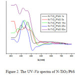 |
Figure 2: The UV–Vis spectra of N-TiO2/PbS 15 immersion cycles. |
The N-TiO2 gives only the absorption value in the UV region (λ <375 nm). Whilst the N-TiO2/PbS systems indicate absorption shifting towards the visible light. This increases the optical absorption intensity due to the sensitization of PbS on the N-TiO2, and the absorptions undertake at wavelengths greater than 400 nm. The N-TiO2/PbS provides the change of electronic transition to the UV region as well as to the visible light (Table 2).
Table 2: Absorbances the N-TiO2/PbS
|
Sample |
l Visible (nm) |
l UV (nm) |
d-d (nm) |
π → π* (nm) |
|
N-TiO2/PbS (1x) |
525 |
363, 301 |
363 |
– |
|
N-TiO2/PbS (5x) |
495 |
294, 340 |
340 |
294 |
|
N-TiO2/PbS (15x) |
588 |
270, 334 |
334 |
270 |
|
N-TiO2/PbS (25x) |
613 |
320 |
320 |
– |
|
N-TiO2/PbS (50x) |
536 |
244, 319 |
319 |
244 |
The changes of electronic transition occur in UV and visible areas. The samples of N-TiO2/PbS immersed 5, 15, and 50 cycles provide the maximum absorbances of 294 nm, 270 nm, and 244 nm, respectively, indicating intraligand transitions π→π*. Intraligand transitions π→π* occured due to the presence of nitrogen atoms in TiO2 laticces. According to Asahi et al. the doped nitrogen in the TiO2 matrix can alter the structure of the electronic band of titania by combining the 2p nitrogen and 2p oxygen (N 2p and O 2p → Ti dxy) orbitals, thus shortening the bandgap energy of the TiO2 material significantly.8,18 The presence of the intraligand transition π→π* indicates that nitrogen is being doped in TiO2.
The N-TiO2/PbS immersed by 1, 5, 15, 25, and 50 cycles show the maximum absorbances of 363 nm, 340 nm, 334 nm, 320 nm, and 319 nm, respectvely, indicating an overlapping metal-ligand charge transfer (MLCT) electronic transition (d→d transition). The samples also show several electronic transitions in visible light areas giving the maximum absorbances of 525 nm, 495 nm, 588 nm, 613 nm, and 536 nm, which also indicate a MLCT.19,20
The Kubelka–Munk function was used to calculate the band gap energies of the samples by plotting [F(R’∞)·hυ]1/2 versus energy of light.21,22 The selected graphs are presented in Figure 3a and 3b, The band gaps energies of the samples are tabulated in Table 3. The band gap energies are 2.14 and 3.49 eV, and 3.50 eV for N-TiO2 and TiO2, respectively, revealing that the band gap of TiO2 was narrowed by N doping. In this work, the band gap narrowing may be caused by the introduction of nitrogen from ethylenediamine into the lattice of TiO2. Therefore, it can be concluded that the sample of N-TiO2may exhibit high photocatalytic activity under visible-light irradiation.23,24
The band gap energies of the N-TiO2/PbS are listed in Table 3. The pure N-TiO2 material produces two band gap energies of about 2.14 eV (Eg1) and 3.49 eV (Eg2) while the N-TiO2/PbS has Eg1 and Eg2 about 1.63 eV and 3.07 eV, repectively. The Eg1 is steady along with the increasing of cycles, while Eg2 decreases. A significant decrease of Eg2 occurs after sensitization of the N-TiO2 thin layer using PbS. The PbS sensitization of TiO2 thin layer also increases the device voltage by pressing the thin layer TiO2 surface.25,26 Increasing the device voltage will decrease the distance between the conduction band gap and the valence band.
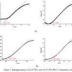 |
Figure 3: Bandgap energy of (a) N-TiO2, and (b) N-TiO2/PbS 15 immersion cicles. |
Table 3: Band gap energies of N-TiO2/PbS
| Samples | Band gap energy (eV) | |
| Eg1 | Eg2 | |
| TiO2 (anatase) | – | 3.50 |
| N-TiO2 | 2.14 | 3.49 |
| N-TiO2/PbS (1 cycle) | 1.64 | 3.07 |
| N-TiO2/PbS (5 cycles) | 1.63 | 3.07 |
| N-TiO2/PbS (15 cycles) | 1.63 | 3.07 |
| N-TiO2/PbS (25 cycles) | 1.63 | 3.04 |
| N-TiO2/PbS (50 cycles) | 1.63 | 2.78 |
Characterization using the SEM method was performed to study the morphology of N-TiO2 and N-TiO2/PbS samples. The pure N-TiO2 consists of irregular shape particles with sizes of 1 to 2.5 µm (Figure 3.a). The N-TiO2/PbS samples indicate two different morphologies, ie. irregular and regular in shapes. The exixtence of regular shaped particles allegedelly as PbS are more dominant in sample with more cycles. The SEM micrograph of N-TiO2/PbS with 50 cycles can be seen in Figure 3.b. The sample consists of irregular shaped particles with the size varies between 1 to 2.5 µm, and the regular shaped having size of about 5 µm.
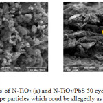 |
Figure 4: SEM micrographs of N-TiO2 (a) and N-TiO2/PbS 50 cycles (b). Yellow arrows are pointing regular shape particles which coud be allegedly as the crystalline PbS. Click here to View figure |
Conclusions
The N-TiO2 PbS crystallites have the size of about 6.05-8.06 nm, dominated by the structures of N-TiO2 anatase and PbS cubic.The immersion cycles of N-TiO2 in the PbS deposition solution do not significantly affect the band gap energies, however the PbS sensitization to the N-TiO2 by the SILAR method decreases the band gap energies.
References
- International Renewable Energy Agency (IRENA), Technology Roadmap., 2018.
- Chwieduk, D., Solar Energy in Buildings. , 2014, 21, 62.
- Sampaio, P.G.V.; Gonzalez, M.O.A., Renew. Sustain. Energy Rev., 2017, 74, 590-601.
CrossRef - Español, P.; Serrano, M.; Pagonabarraga, I; Zúñiga, I., Soft Matter., 2016, 12, 4821-4837.
CrossRef - Kim, Y.H.; Kwon, S.G.; Sung, M.J.,. Repub. Korean Kongkae Taeho Kongbo., 2017, -, 28.
- Xu, W.; Tan, F.; Liu, X.; Zhang, W.; Qu, S.; Wang, Z.; Wang, Z., Nanoscale Res. Lett., 2017, 12, -.
- Son, D.-Y.D.D.-Y.D.D.-Y.; Im, J.-H.J.J.-H.J.; Kim, H.-S.H.; Park, N.-G.N.N.-G., J. Phys. Chem. C., 2014, 118, 16567-16573.
CrossRef - Asahi, R.; Ohwaki; Taoki; Ktaga, Y., Science, 2001, 293, 269-271.
CrossRef - Zhang, Z.-L.; Li, J.-F.; Wang, X.-L.; Qin, J.-Q.; Shi, W.-J.; Liu, Y.-F.; Gao, H.-P.; Mao, Y.-L., Nanoscale Res. Lett., 2017,12, 43.
CrossRef - Kushwaha, R; Chauhan, R.; Srivastava, P.; Bahadur. L., J. Solid State Electrochem., 2015, 19, 507-517.
CrossRef - Liu, J.; Gao, C.; Luo, L.; Ye, Y.Q.; He, X.; Ouyang, L.; Guo, X.; Zhuang, D.; Liao, C.; Mei, J.; Lau, L.; Woon, M., J. Mater. Chem. A., 2015, 3, 28-30.
- Zhou, W.; Yu, C.; Fan, Q.; Wei, L.; Chen, J.; Yu, J.C., Cuihua Xuebao/Chinese J. Catal. 2013, 34, -.
- Wang, Y.; Li, J.; Xue. C.; Zhang, Y.; Jiang, G.; Liu, W.; Zhu, C., Electron. Mater. Lett., 2017, 13, 478-482.
CrossRef - Mamiyev, Z.Q.; Balayeva, N.O., Opt. Mater. (Amst), 2015, 46, 522-525.
CrossRef - Suganya, M.; Balu, A.R., Mater. Sci., 2017, 35, -.
- Smilgies, D.-M. et al,. J. Appl. Crystallogr., 2009, 42, 1030-1034.
CrossRef - Popa, A.; Lisca, M.; Stancu, V.; Buda, M.; Pentia, E.; Botila, T., Journal of Optoelectronics and Advanced Materials., 2006, 8, 43-45.
- Asahi, R.; Morikawa, T., Chem. Phys., 2007, 339, 57-63.
CrossRef - Wang, S.; Yu, Z.C.; Han, L.; Dai, C.L.; Song, J.Y., Asian J. Chem., 2012, 24, 214-216.
- Harris, J.A.; Trotter, K.; Brunschwig, B.S., J. Phys. Chem. B., 2007, 111, 6695-6702.
CrossRef - Lin, H.; Huang, C.P.; Li, W.; Ni, C.; Ismat, S.S.; Tseng ,Y.-H., Appl. Catal. B Environ., 2006, 68, 1-11.
CrossRef - Ahsan, R.; Khan, M.Z.R.; Basith, M.A., J. Nanophotonics., 2017. 11, -.
- Liu, C.; Zhang, L.; Liu, R.; .Gao, Z.; Yang, X.; Tu, Z.; Yang, F.; Ye, Z.; Cui, L.; Xu, C.; Li, Y., J. Alloys Compd., 2016, 656, 24-32.
CrossRef - Tang, R.; Jiang, Q; Liu, Y., Procedia Eng., 2017, 205, 573-580.
CrossRef - Cai, F.; Yang, F.; Zhang, Y.; Cai, F.; Yang, F.; Zhang, Y.; Ke, C.; Cheng, C.; Zhao, Y.; Yan, G., Phys. Chem. 2014, 16, 23967-23974.
- Basit, M.A.; Abbas, M.A.; Jung, E.S.; Park, Y.M.; Bang, J.H.; Park, T.J., Electrochim. Acta., 2016, 211, 644-651.
CrossRef

This work is licensed under a Creative Commons Attribution 4.0 International License.
![]()
A New Edition of Web of Science
Journal Impact Factor
2022: 0.5
Five Year: 0.8
Journal is Indexed in

Cabells Whitelist
![]()


