Investigation on Al Doped Zno Thin Films and its N-Alzno/P-Si Junction Diodes Via Dip Coating and JNSP Techniques
S. Kalidass1,2, P. Thirunavukkarasu1 , M. Balaji3 and J. Chandrasekaran4
1Department of Electronics, Sri Ramakrishna Mission Vidyalaya College of Arts and Science, Coimbatore 641020, Tamil Nadu, India.
2Department of Electronics Department of Electronics,Government Arts College, Trichirapalli -620022, Tamil Nadu, India.
3Department of Physics, Bannari Amman Institute of Technology, Sathyamanglam, Tamil Nadu 638401, India.
4Department of Physics, Sri Ramakrishna Mission Vidyalaya College of Arts and Science, Coimbatore 641020, Tamil Nadu, India.
Corresponding Author E-mail: iruarasu@yahoo.co.in
DOI : http://dx.doi.org/10.13005/ojc/340548
Article Received on : 20-06-2018
Article Accepted on : 27-08-2018
Article Published : 09 Oct 2018
From this investigation, we find out that the dip coating and jet nebulizer spray pyrolysis (JNSP) techniques are the suitable to fabricate aluminum doped zinc oxide (AlZnO) thin films and the P-N junction diode of n-AlZnO/p-Si at 450°C. Several characterization techniques are used to measure the consequences of Al doping (0, 0.5, 1.0, 1.5, 2.0 and 2.5 wt.%) on structural, optical, electrical and diode properties of ZnO. We recorded that the films were polycrystalline with a hexagonal structure of ZnO by the X-ray diffraction (XRD) analysis. The disparities of the sub-micro sized rod-like structures are observed from the scanning electron microscope (SEM) images. The energy dispersive X-ray spectroscopy (EDX) analysis proved that the elements of Al, Zn and O were presented in the film. The absorbance and band gap energy (Eg) values were ascertained from the ultraviolet visible (UV-vis) analysis. By the current-voltage (I-V) characterization, the maximum conductivity value is detected for 1.5 wt.% of Al doped ZnO film. The I-V measurement for finding the diode parameters of ideality factor (n) and barrier height (Fb) in dark and under light was taken.
KEYWORDS:AlZnO Thin Films; Dip Coating; JNSP Technique; P-N Junction Diode
Download this article as:| Copy the following to cite this article: Kalidass S, Thirunavukkarasu P, Balaji M, Chandrasekaran J. Investigation on Al Doped Zno Thin Films and its N-Alzno/P-Si Junction Diodes Via Dip Coating and JNSP Techniques. Orient J Chem 2018;34(5). |
| Copy the following to cite this URL: Kalidass S, Thirunavukkarasu P, Balaji M, Chandrasekaran J. Investigation on Al Doped Zno Thin Films and its N-Alzno/P-Si Junction Diodes Via Dip Coating and JNSP Techniques. Orient J Chem 2018;34(5). Available from: http://www.orientjchem.org/?p=50410 |
Introduction
Nowadays, forming a p-n junction diode by transition metal oxide (TMO) as an n-type layer and silicon (Si) wafer as a p-type is convincing method for electronics industry. The recent survey concludes that the some TMOs of MoO3, WO3, ZnO and NiO1 are widely used. Among these TMOs, ZnO has a wide band gap energy and it has required structural and electronic properties. Moreover, ZnO has been played a vital role in various applications of UV lasers and short-wavelength optoelectronic device.2,3 Besides ZnO can be apt in the applications of photoconductors,4 gas sensors5 and photovoltaic.6 ZnO films can be grown using the following techniques such as thermal evaporation, spray pyrolysis, chemical vapour deposition, dip coating, etc., and.7-14 Among them dip coating method was chosen from the list for preparing thin films and JNSP technique15,16 was opted for preparing P-N junction diodes.
From this work, AlZnO thin films and n-AlMoO3/p-Si junction diodes with different doping concentrations of Al (0, 0.5, 1.0, 1.5, 2.0, 2 and 2.5 wt. %) were developed at a annealed temperature of 450°C by dip coating practiceand the diodes were groomed using JNSP technique. The structural, electrical and optical properties were obtained for dip coated ZnO films. From I-V measurement, the diode parameters of n and Fb were calculated for n-AlMoO3/p-Si junction diodes in dark and under light.
Experimental Conditions
Fabrication of AlZnO films and n-AlMoO3/p-Si diode
The starting solution was prepared with 0.10 M of zinc acetate and aluminium acetate (0, 0.5, 1.0, 1.5, 2.0 and 2.5 wt.%) in 100 ml of ethanol and stirred for 45 min. Mono ethylamine (MEA) was added into the starting solution for ionizing and stirred for an hour. The well cleaned slide was dipped into the prepared solution and deionized water simultaneously for 30 seconds of 5 times. The deionized water was kept at 85°C. After that, the prepared slides were annealed at 450°C. Initially, the Si wafer cleaning is indispensable to construct a quality PN junction diode because there may be some impurities of dust, grease and organic residues present on the surface. A detailed study of steps involving in cleaning process has been known in a publication [16]. Using JNSP technique at 450°C, the p-type Si wafer (1 x 1 cm size) was coated with 1.5ml of starting solution by spray method. The Silver (Ag) paste was applied and dried for 5 h at ambient condition to both surfaces of the prepared n-AlZnO /p-Si diode for getting a better electrical contact owing to its notable properties of adhesion, electrical conductivity, low sheet resistance (>0.02 Ω/cm) and good solderability. The JNSP technique was used to fabricate diodes and the details are illustrated in some publications.15,16
Characterization Techniques
The XPERT-PRO X-ray diffractometer (XRD) is fixed in the angle of diffraction (2θ) range of 20 to 70°C with CuKα1 radiation of wavelength 1.5406 Å to measure the 2θ peaks which will be used to obtain the structural properties of the prepared thin films. JEOL JEM 2100 scanning electron microscope (SEM) was used to image the surface morphology of the prepared films. The QUANTA FEG 250 energy dispersive X-ray spectroscopy (EDX) is helps to prove the presence of elements of Al, Zn and O in the prepared films. Using Perkin Elmer Lambda 35 UV-visible spectrophotometer (UV-vis), the optical properties were explored in the visible region. Keithley Electrometer 6517-B was used to perceive the electrical properties and diode parameters of the AlZnO films and n-AlMoO3/p-Si diode.
Results and Discussion
XRD Pattern
The XRD pattern for various wt.% of Al doped ZnO films prepared at a sample temperature of 450ºC noticeable all around air is appeared in Figure 1. The Figure 1 indicates the prepared Al doped ZnO films are polycrystalline with hexagonal structure of ZnO (JCPDS-Card No. 89-0510) for a favored orientation along (1 0 1) and other XRD crests at (0 0 2) and (1 0 0) planes. Likewise, Figure 1, deciphers that no different phases typically identified from dip coated AlZnO films at 450ºC because of (i) the base measure of Al element may display as little bunches in ZnO lattices, thus, it may be extremely hard to distinguish by XRD and (ii) most likely put in the grain boundaries of the ZnO nanocrystals – or dispersed atomically in the ZnO lattice.17-19
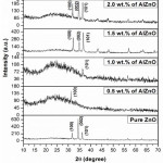 |
Figure 1: XRD pattern of Al doped ZnO thin filmsfor different concentrations of Al. |
From Table 1, the structural parameters of AlZnOfilms for the chosen direction of (0 4 0) plane. The parameters of crystallite size (D),20 microstrain (ε), dislocation density (δ) and stacking fault (SF) can be found the following relations (1-4).16
where k, λ, θ and β are the shape factor, wavelength of the X-ray radiation, diffraction angle and full width at half maximum.
Table 1: Structural parameters of Al doped ZnO films for different doping concentrations of Al.
|
Al doping (wt.%) |
Crystallite size (D) (nm) |
Micro strain (ε) (x 10-3 lines-2 m-4) |
Dislocation density (x 1014 cm-2) |
Stacking Fault (x 10-2) |
|
0 |
56.411 |
0.6149 |
3.1424 |
0.1619 |
|
0.5 |
56.420 |
0.6113 |
3.1072 |
0.1597 |
|
1.0 |
56.510 |
0.6095 |
3.0964 |
0.1579 |
|
1.5 |
56.605 |
0.5908 |
2.9986 |
0.1454 |
|
2.0 |
53.31 |
0.6507 |
3.5185 |
0.1403 |
|
2.5 |
41.43 |
0.8371 |
5.8211 |
0.1816 |
The D values from 56.51 to 41.43 nm of the chosen direction (0 4 0) plane is obtained by Al concentration increment from 0 to 2.5 wt.%. Microstrain, dislocation density and stacking fault values have changed with increasing of concentration (Table 1).21,22
SEM Analysis
Figure 2a-f illustrates the morphological images of the prepared AlZnO thin films for different concentrations (0, 0.5, 1.0, 1.5, 2.0 and 2.5 wt.%) of Al. The hexagonal faced rod-like structures with random in alignment are found to pure ZnO (Figure 2a&b). The concentration of Al from 1.0 to 2.0 wt.% portrays the randomly arranged micro-rod like structures (Figure 2c-e). 2.5 wt.% of Al doped ZnO film exhibits the agglomeration in grains, which shows hasty disparity nature of rods compare to low concentrations of Al doped ZnO films (Figure 2f). It results that the surface morphology of the dip coated AlZnO films remarkably varied by Al concentrations.
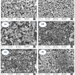 |
Figure 2: SEM images of Al doped ZnO thin films for different concentrations of a) 0, b) 0.5, c) 1.0, d) 1.5, e) 2.0 and f) 2.5 wt.% of Al. |
EDX Spectra
The EDX spectra of the dip coated AlZnO thin films for various concentrations (0, 0.5 and 2.5 wt.%) of Al is shown in Figure 3. The elements of Al, Zn and O with no additional elements present in the dip coated AlZnO films were confirmed by the EDX spectra. The increasing of Al concentrations results that the atomic ratio of Al in increased.
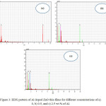 |
Figure 3: EDX pattern of Al doped ZnO thin films for different concentrations of a) 0, b) 0.5, and c) 2.5 wt.% of Al. |
Table 2: Atomic ratio for Al doped ZnO thin films.
|
Al doping concentration (wt.%) |
Atomic ratio (%) |
||
|
Al |
Zn |
O |
|
|
0 |
0 | 55.10 | 44.90 |
|
0.5 |
1.04 | 51.20 | 47.76 |
|
2.5 |
2.14 | 51.06 | 48.80 |
UV-vis Spectroscopy
From Figure 4, the absorbance spectra depicts the dip coated pure ZnO and Al doped ZnO films prepared at 450ºC of sample temperature. From the Figure 4, the absorbance values slightly varied by increasing the concentration of Al. Among the different concentrations of Al with ZnO films except pure ZnO, 1.5wt% of Al doped ZnO is recorded with minimum absorbance value. The concentration of Al varies the density of unsaturated bonds which results the changes in absorbance. In general, transmission from valance to conduction band states the optical absorbance but absorption in visible range suggests the unchanged localized energy states in band gap.23
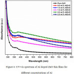 |
Figure 4: UV-vis spectrum of Al doped ZnO thin films for different concentrations of Al. |
Eg values of the AlZnO films have been calculated by UV-vis spectra with the following eqn. (5),16,24
![]()
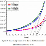 |
Figure 5: Band energy values of Al doped ZnO thin films for different concentrations of Al. |
Plot of (ahν)2 Vs. (αhν) for different concentrations of Al doped ZnO films is drawn as shown in Figure 5. The direct band gap nature of prepared AlZnO films is identified by straight line portion of the plot. Eg values of 3.03 eV for the undoped ZnO film and 3.00, 2.90, 3.20, 2.80 and 2.94 eV for various concentrations (0.5, 1.0, 1.5, 2.0 and 2.5 wt. %) of Al doped ZnO was attained by extrapolating a line to the axis of hν. 1.5 wt.% of Al doped ZnO reveals maximum Eg values compare to other doping concentrations of Al doped ZnO films except pure one. The variation in Eg may be due to the increasing of defects in structural parameters while preparing the AlZnO films.24
Current (I) – Voltage (V) characterization
I-V characterization of electrical conductivity (s)
The I-V measurement was noted at ambient condition for the prepared AlZnO films for different concentrations of Al by Keithley electrometer 6517-B. The applied voltage is 10 – 100 V (increasing of of 10 V) on the prepared thin films and its corresponding current flow is measured. The I-V plot of AlZnO thin films for various concentrations (0, 0.5, 1.0, 1.5, 2.0 and 2.5 wt.%) of Al is displayed in Figure 6. The values of current are considerably changed for increasing Al concentration with its respective applied voltage (Figure 6).
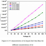 |
Figure 6: I-V characteristics of Al doped ZnO thin films for different concentrations of Al. |
The s value has been attained using the given eqn. (6),16
![]()
where I, V, d, and A are the current, applied voltage, inter-probe distance and cross-sectional area of the film.
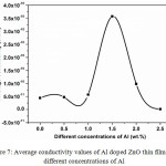 |
Figure 7: Average conductivity values of Al doped ZnO thin films for different concentrations of Al. Click here to View figure |
The Average conductivity (σavg) values of AlZnO films varied by increasing the concentration of Al (Figure 7). The σavg values for pure ZnO and 0.5, 1.0, 1.5, 2.0 and 2.5 wt.% of Al doped ZnO are 4.464 x 10⁻¹¹, 4.751 x 10⁻¹¹, 5.731 x 10⁻¹¹, 3.575 x 10⁻¹⁰, 9.811 x 10⁻¹¹ and 1.588 x 10⁻¹² S/cm (Figure 7). From the results, 1.5 wt.% Al doped ZnO reveals the maximum σavg value. The obtained results might be due to the oxygen vacancies25-27 of AlZnO films.
I-V characterization of n-AlZnO/p-Si diode
The prepared n-AlZnO/p-Si junction diodes for pure and 1.5 wt.% of Al doped ZnO were studied as shown in Figure 8a&b and the parameters of n and Fb values in dark and under light were calculated. Figure 9a&b indicates the semi-log plot of current density (ln J) Vs. voltage (V). The voltage of reverse to forward bias from -4 to +4 V was applied and its corresponding current value is measured which indicates a good rectification of n-AlZnO/p-Si junction diodes.
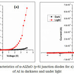 |
Figure 8: I-V characteristics of n-AlZnO /p-Si junction diodes for a) 0 and b) 1.5 wt.% of Al in darkness and under light. |
The J values for the prepared n-AlZnO/p-Si junction diodes have been calculated using the thermionic emission theory (TE) as given below eqn. (7).28
![]()
where Jo, q, V, n, K and Tis the reverse saturation current density, electron charge, applied voltage, ideality factor, K Boltzmann constant and absolute temperature.
The n value and Fb have been calculated using the eqns. (8,9).29
where A* is the Richardson constant.
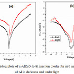 |
Figure 9: Semi-log plots of n-AlZnO /p-Si junction diodes for a) 0 and b) 1.5 wt.% of Al in darkness and under light. |
From calculated values, the n values for pure and 1.5% Al doped n-ZnO/p-Sidiodes are 4.08 and 4.34 in darkness but under the light, it decreases into 3.32 and 3.69. The variation in n values might be due to the absorption of prepared AlZnO thin films with its thickness and also might be due to the conversion efficiency of Si wafer.30 The n values of the prepared n-ZnO/p-Si diodes are higher than the ideal value of one which indicates the non-ideal behavior of prepared diodes. The reasons may be owing to the occurrence of interfacial thin oxide (SiO2) layer between electrode of Ag and Si wafer or the recombination of current or bias dependent Fb.31 Additional causes might be owing to defects of the states on the surface of the semiconductor,32,33 chemical reactions and barrier inhomogeneities.34
Conclusion
The preparation of AlZnO films for various concentrations (0, 0.5, 1.0, 1.5, 2.0 and 2.5 wt.%) of Al at the annealing temperature of 450°C using dip coating method. XRD pattern shows that the dip coated AlZnO films exhibited a hexagonal structure and D is varied from 41.43 to 56.61 nm as increase in Al concentrations. From SEM result, the surface morphology is vastly disturbed by the concentration of Al. The confirmation of Al, Zn and O element existence in the present work is observed by EDX analysis. In UV-vis analysis, the 1.5 wt.% Al doped ZnO film gives a minimum absorbance value compared to other doping concentrations of Al and Eg value was changed from 2.80 to 3.03 eV. I-V characteristic reveals that a maximum s of 3.575 x 10⁻¹⁰ S/cm was reached for 1.5 wt.% Al doped ZnO film. The JNSP technique is used to the prepare n-ZnO/p-Si diodes for various concentrations (0 and 1.5 wt.%) of Al at the sample temperature of 450°C. the minimum n values of 3.32 and 3.69 for pure and 1.5 wt.% n-AlZnO/p-Si diode under light.
Acknowledgement
The authors gratefully acknowledge Dr. N. Anandhan, Alagappa University, Karaikudi, Dr. V. Manickam, St. Joseph’s College (Autonomous), Tiruchirapalli and ARIC, SRMV College of Arts and Science, Coimbatore, for providing instrumentation facilities.
References
- Bao, D.; Gu, H.; Kuang, A. Thin Solid Films 1998, 312, 37-39.
CrossRef - Dong, H.; Zhou, B.; Li, J.; Zhan, J.; Zhang, L. J. Materiomics 2017, 3, 255-266.
CrossRef - Ohshima, T.; Ikegami, T.; Ebihara, K.; Thareja, R.K. Electrical Engineering in Japan, 2002, 122-A, 689-694.
- Haga, Y.; Inoue, S.; Sato, T.; Yosomiya, R. Angew. makromol. chem. 1986, 139, 49-61.
CrossRef - Balram, D.; Lian, K.Y.; Sebastian, N. Int. J. Electrochem. Sci. 2018, 13, 1542-1555.
CrossRef - Dumbrava, A.; Prodan, G.; Moscalu, F.; Mater. Sci. Semicond. Process. 2013, 16, 1095-1104.
CrossRef - Manzi, J.A.; Knapp, C.E.; Parkin, I.P.; Carmalt, C.J. Eur. J. Inorg. Chem. 2015, 3658–3665.
CrossRef - Shanmugasundaram, K.; Thirunavukkarasu, P.; Ramamurthy, M.; Balaji, M.; Chandrasekaran, J. Orient. J. Chem. 2017, 33, 1-7.
CrossRef - Dumbrava, A.; Prodan, G.; Moscalu F. Mater. Sci. Semicond. Process. 2013, 16, 1095-1104
CrossRef - Alfaro Cruz, M.R.; Ortega Zarzosa, G.; Martinez Castanon, G.; Martinez, J.R. Mater. Lett. 2012, 78, 159-161.
CrossRef - Bhattacharyya, P.; Basu, P.K.; Saha, H.; Basu, S. Sens. Actuators B 2007, 124, 62-67.
CrossRef - Lupan, O.; Pauporte, T.; Chow, L.; Viana, B.; Pelle, F.; Ono, L.K.; Roldan Cuenya, B.; Heinrich, H. Appl. Surf. Sci. 2010, 256, 1895-1907.
CrossRef - Zhao, L.; Lian, J.; Liu, Y.; Jiang, Q. Appl. Surf. Sci. 2006, 252, 8451-8455.
CrossRef - Thambidurai, M.; Muthukumarasamy, N.; Velauthapillai, D.; Lee, C. J. Mater. Sci: Mater. Electron. 2012, DOI 10.1007/s10854-012-1035-8.
CrossRef - Sethupathi, N.; Thirunavukkarasu, P.; Vidhya, V.S.; Thangamuthu, R.; Kiruthika, G.V.M.; Perumal, K.; Bajaj, H.C.; Jayachandran, M.J. Mater. Sci. Mater. Electron. 2012, 23, 1087-1093.
CrossRef - Balaji, M.; Chandrasekaran, J.; Raja, M. Mater. Sci. Semicond. Process. 2016, 43, 104-113.
CrossRef - Song, X.C.; Yang, E.; Liu, G.; Zhang, Y.; Liu, Z.S.; Chen, H.F.; Wang, Y. J. Nanopart. Res. 2010, 12, 2813.
CrossRef - Reddy, A.S.; Figueiredo, N.M.; Cho, H.C.; Lee, K.S.; Cavaleiro, A. Mater. Chem. Phys. 2012, 133, 1024.
CrossRef - O-Rueda de Leon, J.M.; Acosta, D.R.; Pal, U.; Castaneda, L. Electrochim. Acta 2011, 56, 2599.
- Scherrer, P. Nachr. Ges. Wiss. Gottingen. 1918, 26, 98.
- Madhavi, V.; Kumar, P.J.; Kondaiah, P.; Hussain, O.M.; Uthanna, S. Ionics 2014, DOI:10.1007/s11581-014-1073-8.
CrossRef - Lethy, K.J.; Beena, D.; Pillai, V.P.M.; Ganesan, V. J. Appl. Phys. 2008, 104, 033515.
CrossRef - Mishra, R.K.; Sahay, P.P. Mater. Res. Bull. 2012, 47, 4112.
CrossRef - Luo, Y.; Yin, B.; Zhang, H.; Qiu, Y.; Lei, J.; Chang, Y.; Zhao, Y.; Ji, J.; Hu, L. J. Mater. Sci.: Mater. Electron. 2016, 27, 2342.
CrossRef - Nirupama, V.; Chandrasekhar, M.; Radhika, P.; Sreedhar, B.; Uthanna, S. J. Optoelectron. Adv. Mater. 2009, 11, 320.
- Nirupama, V.; Chandrasekhar, M.; Subramanyam, T.K.; Uthanna, S.; J. Phy.: Conf. Ser. 2010, 208, 012101.
CrossRef - Sutrave, D.S.; Gothe, S.D. Int. Sci. J. 2015, 2, 2348.
- Sze, S.M. Semiconductor Devices, 2nd ed. (Wiley, New York,), 2001, p. 224
- Ugurel, S.A.E.; Serifoglu, K.; Turut, A. Microelectron. Eng. 2008, 85, 2299.
CrossRef - Canfield, L.R.; Vest, R.; Woods, T.N.; Korde, R. Ultraviolet Tech. V 1994, 2282, 31.
CrossRef - Padma, R.; Nagaraju, G.; Rajagopal Reddy, V.; Choi, C.J. Thin Solid Films 2015, DOI:10.1016/j.tsf.2015.12.018
CrossRef - Dogan, H.; Yildrim, N.; Turut, A. Microelectron. Eng. 2008, 85, 655.
CrossRef - Sze, S.M. Physics of Semiconductor Devices, 2nd edn. (Wiley, New York, 1981)
- Rhoderick, E.H.; Williams, R.H. Metal-semiconductor Contacts (Clarendon Press, Oxford, 1988).

This work is licensed under a Creative Commons Attribution 4.0 International License.
![]()
A New Edition of Web of Science
Journal Impact Factor
2022: 0.5
Five Year: 0.8
Journal is Indexed in

Cabells Whitelist
![]()


