Structural, Morphological and Optical Properties of aluminium doped ZnO Thin Film by Dip-Coating Method
Ba. Anandh1 , A. Shankar Ganesh1, R. Thangarasu2, R. Sakthivel3, R. Kannusamy4 and K. Tamilselvan5
1,3, 4.5Department of Electronics, PSG College of Arts and Science, Coimbatore-14, India.
2Department of Physics, PSG College of Arts and Science, Coimbatore-14, India.
Corresponding Author E-mail: anandh.ba@gmail.com
DOI : http://dx.doi.org/10.13005/ojc/340356
Article Received on : January 23, 2018
Article Accepted on : May 18, 2018
Article Published : 29 May 2018
Dip coating method is used for depositing Aluminium (Al) doped Zinc Oxide (ZnO) thin films on glass substrate. Undoped, 1%, 3% and 5% Al doped ZnO thin films are prepared and their structural, morphological and optical properties are studied. X-ray diffraction study confirms that films are polycrystalline with hexagonal arrangement. Field Emission Scanning Electron Microscope (FESEM) is used to analyze the surface morphology and it shows the spherical like structure. Energy Dispersive X-ray Analysis (EDX) pattern shows the presence of Zn, O and Al. UV-Vis. Spectroscopy and Photoluminescence spectroscopy (PLS) are used to study optical properties. Optical study indicates that both undoped and Aluminium doped ZnO films are transparent in UV region and closer to visible region. The band gaps of the films are 3.55eV, 3.68eV, 3.82eV and 3.25eVfor undoped, 1%, 3% and 5% Aluminium doped ZnO films correspondingly.
KEYWORDS:Aluminium Doped ZnO; Dip Coating; Field Emission Scanning Electron Microscope (FESEM); Photoluminescence Spectroscopy (PL); Spectroscopy (UV); Thin Film; UV-Vis; X-ray Diffraction (XRD)
Download this article as:| Copy the following to cite this article: Anandh B. A, Ganesh A. S, Thangarasu R, Sakthivel R, Kannusamy R, Tamilselvan K. Structural, Morphological and Optical Properties of aluminium doped ZnO Thin Film by Dip-Coating Method. Orient J Chem 2018;34(3). |
| Copy the following to cite this URL: Anandh B. A, Ganesh A. S, Thangarasu R, Sakthivel R, Kannusamy R, Tamilselvan K. Structural, Morphological and Optical Properties of aluminium doped ZnO Thin Film by Dip-Coating Method. Orient J Chem 2018;34(3). Available from: http://www.orientjchem.org/?p=46214 |
Introduction
Transparent conductive oxide (TCO) materials have many applications in the area of displays, photovoltaic devices and LED’s[1-3].Zinc oxide has extensive band gap (3.37eV) at room temperature, good chemical stability, excellent thermal stability and high exciting binding energy (60meV)[4]. ZnO thin films have many advantages such as non-toxic, low cost, good electrical and optical properties with very high electrical resistivity [5].The properties of ZnO films can be improved by doping any one of the group III element. Aluminium is one of the group III element which is mainly doped with ZnO to obtain good stability and low resistivity [6].
Many methods were used to obtain ZnO thin films such as chemical bath deposition [7], dip coating method [8], thermal vacuum evaporation method [9], sol-gel method [10], hydrothermal method [11], magnetron sputtering [12], oxygen plasma assisted molecular beam epitaxy [13], laser coating and several other methods. Dip coating method is simple, inexpensive and gives uniform thin films.
The aim of the present work is to study the effect of aluminium doping on structural, morphological and optical properties of ZnO thin films.
Experimental Procedure
Cleaning of Glass Substrate
The glass substrates for depositing the films are initially cleaned with detergent, DI water and acetone. Nitric acid and DI water are used for secondary cleaning process and finally the glass substrates are cleaned in ultrasonic bath using acetone and dried for 10 minutes in hot air oven.
Deposition of undoped ZnO and Aluminium (Al) doped ZnO thin films
Zinc acetate dehydrate (ZAD) is used as base material. Ethanol and Monoethanolamine were used as solvent and stabilizer respectively. The zincate bath was prepared and dissolving ZAD in 100ml of ethanol and stirred for 2 hours using magnetic stirrer and left covered for 24 hours. Molar ratio between ZAD and MEA is kept at 0.1M. The undoped ZnO film is prepared by alternatively dipping the precleaned glass substrate into zincate and hot DI water baths for 30 sec each and the dipping process is repeated for 30 cycles.
Aluminium acetate is used for doping aluminium and is added along with ZAD in 100 ml and ethanol is stirred for 2 hours in magnetic stirrer and kept covered for 24 hours. The solutions are prepared for 1%, 3% and 5% Al content. Al doped ZnO films are formed by alternately dipping the pre-cleaned microscopic glass substrate in Al dissolved zincate bath and hot DI water bath for 30 sec each and the dipping process is repeated for 30 cycles. The ZnO films are prepared for undoped, 1%, 3% and 5% Al content and post annealed at 350˚C.
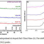 |
Figure 1a: XRD of undoped and Al doped ZnO Thin Films (b) The shift position in the diffraction angles at (002) peaks.
|
Resluts and Discussion
Structural Studies
Figure 1(a) represents XRD of undoped, 1%, 3%, and 5%Al concentrations of ZnO films, post annealed at 350ºC.The peaks appeared in the XRD pattern shows the Wurtzite hexagonal form of ZnO (JCPDS card: 89-1397). The orientation of peak at (002) plane shows the polycrystalline nature, other XRD peaks appear at (100), (101), (102), (110), (103) and (112) planes. Fig.1 (b) shows change in lower diffraction angle (33.5º to 33.5º) for different peaks owing to the Al concentration. The intensity of the peak in the (002) plane of undoped and Al doped ZnO shows decreased crystal size. The XRD indicates only ZnO peaks and no peaks related to aluminium and its components. The reason may be presence of a small amount of aluminium content in the form of very small cluster in the ZnO lattice, so it may be very hard to detect by XRD instrument and it may present in the grain boundaries of the ZnO nano crystals or distributed atomically within the ZnO lattice.
Debye-Scherrer’s formula [14] is used to calculate the crystalline size of the prepared films.
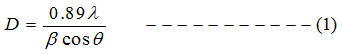
The dislocation density (δ) is calculated using equation 2, and micro strain (ε) values is calculated using equation 3 [15]
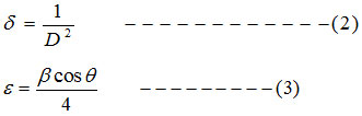
Where D indicates crystalline size, λ for the wavelength, β for the FWHM and θ is the diffraction angle in degrees [16]. Table: 1 indicates that the average crystalline size (D) for undoped ZnO is 31.32nm and it decreases to 16.30nm for 1% Al and 18.66nm for 3% Al and 19.82nm for 5% Al concentration. Micro strain and dislocation density increases with decrease in Al content. Lattice constants ‘a’ and ‘c’ well matches with the standard value.
Table 1: Structural parameters of ZnO thin films for undoped, 1%, 3% and 5% Al content
| Thin Film Sample | 2θ (deg) | (002) inter planer d-spacing distance | FWHM (radians) | Crystalline size(D) | Dislocation Density(δ) | Micro strain (ε) (lines-2 m-4) | Lattice parameters (Aº) | |
| a | c | |||||||
| Undoped ZnO | 34.4299 | 2.60274 | 0.27730 | 31.32 | 1.01908 | 0.001156 | 3.2495 | 5.2082 |
| Al at 1% | 34.5892 | 2.59112 | 0.53300 | 16.30 | 3.76174 | 0.002221 | 3.2399 | 5.1860 |
| Al at 3% | 34.5976 | 2.59051 | 0.46560 | 18.66 | 2.8705 | 0.00194 | 3.2389 | 5.1849 |
| Al at 5% | 34.5831 | 2.59156 | 0.43840 | 19.82 | 2.54505 | 0.001826 | 3.2400 | 5.1871 |
Morphological Studies
The FESEM images of different Al content ZnO thin films are represented in Fig.2. The Spherical shaped particles are seen for undoped, 1% and 3% of Al doped ZnO thin films [17]. Higher concentration of 5% Al doped ZnO thin film shows the large variance in the grains and splitting of spherical shape to rod shape (Fig.2d). The particulate grain almost covers the substrate surface more or less evenly. It is seen that the morphology of ZnO thin films is strongly influenced by aluminium doping.
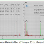 |
Figure 2: FESEM image of ZnO thin films (a) Undoped, (b) 1% Al (c) 3% Al and (d) 5% Al.
|
The EDAX spectrum of undoped and 5% Aluminium doped ZnO thin films are shown in the Fig. 3(a) and 3(b). It confirms Zn, O and Al are present in the prepared film. The atomic percentages of the elements present are given in the insert table of Fig.3.
 |
Figure 3: EDAX spectrum of ZnO thin films (a) Undoped (b) 5% Al doped |
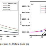 |
Figure 4a: UV Absorption spectrum (b) Optical Band gap
|
Optical Studies
Figure 4(a) shows the UV absorption spectrum of ZnO thin films for undoped and Aluminium doped thin films in the wavelength region 200nm to 1400nm. It shows that minimum absorption seen in 1% Al doped ZnO thin film and the maximum absorbance is seen in 5% Al doped ZnO film. The doping of Al, affects the density of unsaturated bonds causing variation of local states in the band gap and this might be the cause for changes in absorption.
Figure 4(b) shows the relation between (αhυ)2 and (hυ) for undoped and Aluminium doped ZnO thin films. The band gap is obtained from the straight line region of (αhυ)2 versus hυ and the band gap energy of undoped, 1%, 3% and 5% Aluminium doped ZnO thin films are 3.55eV, 3.68eV, 3.82eV and 3.25eV respectively. Fig.4 (b) shows that the band gaps initially widened with increasing aluminium content up to 3% and then the absorption edge shifted again to longer wavelength range [18]. This red shift is clarified by stress relaxation mechanism. This is because impurity band merges into conduction band causing the reduction in the band gap [19].
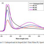 |
Figure 5: Undoped and Al doped ZnO Thin Films PL Spectrum.
|
Figure 5 shows the undoped and Al doped ZnO films PL spectrum for wavelength ranging from 300nm to 550nm under the excitation of 325nm. With increase in the Al doping concentration, the intensity of peak increases with a decrease in peak broadening [20]. The emission spectrum shows two peaks. The strong band emission peak obtained near 381nm relates to near band edge emission of ZnO, the UV emission due to near band edge emission which can be connected to free excitation recombination. The weak band emission peak obtained near 500nm corresponds to green emission peaks associated with deep level emission. The green emission of undoped ZnO has negligible visible peak intensity and as the Al doping content increases the intensity also gets increased. The Al3+ ions can get into the ZnO structures by making oxygen vacancies or incorporating into holes, many of the Al3+ are substituted at low doping concentration and the additional Al3+ incorporate into the gaps of ZnO nano particles at the higher concentration making large amount of lattice defects. The blue green emission peaks are at around 447 nm to 549 nm by the energy transmission of electrons [21].
Conclusion
ZnO thin films are coated on glass substrate for undoped, 1%, 3% and 5% Al content by dip coating method. XRD studies show that the prepared Al-ZnO thin films are polycrystalline nature by Wurtzite hexagonal structure. The crystalline size of the Al doped ZnO films is smaller when matched with undoped ZnO film. By increasing the Al content the crystalline size of the Al doped ZnO thin films get increased. The FESEM analysis shows the spherical growth of undoped and Al doped ZnO thin films. It also shows that surface morphology is strongly disturbed by Al doping. The EDAX result shows the existence of Zn, O and Al elements in the thin films. UV-Vis spectrum shows that least absorbance appears for 1 % Al content in the visible region. The band gap for undoped, 1%, 3% and 5% Al doped ZnO are 3.55eV, 3.68eV, 3.82eV and 3.25eV respectively. Near band emission in the PL spectrum indicates the appearance of interstitial Zn+ ions and deep level emission confirms the oxygen ion vacancy.
Acknowledgement
We are thankful to the Department of Electronics, PSG College of Arts & Science for providing the lab facilities to do our research work and also for taking studies.
References
- Song, J.; Zhou, J.; Wang, A.L.; Nano Lett.,2006, 6, 1656.
CrossRef - Jeong, I.S.; Kim, J.H.; Im, S.; Appl. Phys. Lett., 2003, 83, 2946.
CrossRef - Zhang, Z.Z.; Lu, Y.M.; Shen, D.Z.; Zhang, J.Y.; Li, B.H.; Zhao, D.X.; Fan, X.W.; Tang, K.; Appl. Phys. Lett.,2006, 88, 031911.
CrossRef - Ozgur, U.; AlivovYa, I.; Liu, C.; Teke, A.; Reshchikov, M. A.; Dogan, S.; Avrutin, V.; Cho, S. J.; Morkoc, H. Journal of Applied Physics.2005,98, 041301.
- Hyun, H.M.; Hong, K.; Kim, B.H.; J.Korean Ceram. Soc. 1996, 33, 149-154.
- Majumder, S.B.; Jain, M.; Dobal, P.S.; Katiyar, R.S.; Mater. Sci. Eng., B 2003, 103, 16-25.
CrossRef - Li, Q.W.; Bain, J.M.; Sun, J.C.; Wang, J.W.; Luo, Y.M.; Sun, K.T.; Yu, D.Q.; Appl. Surf. Sci., 2010, 256, 1698.
CrossRef - Boukhenoufa, N.; Mahamdi, R.; Rechem, D. Semicond.2016, 37, 113001.
CrossRef - Meyer, J.; Kidambi, P.R.; Bayer, B.C.; Weijtens, C.; Kuhn, A.; Centeno, A.; Pesquera, A.; Zurutuza, A.; Robertson, J. Sci.Rep.2014,Jun 20, 4:5380.
CrossRef - Prasad, A.K.; Kubinski, D.J. Gouma, P.I.;Sens. Actuators B2003,93, 25.
CrossRef - Yordanov, R.; Boyadjiev, S.; Georgieva, V.; Vergov, L.J.Phys. Conf.Ser.2014, 514, 012040.
CrossRef - Yordanov, R.; Boyadjiev, S.; Georgieva, V.; Vergov, L.J.Phys. Conf.Ser.2014, 514,012040.
CrossRef - Altman, E.I.; Droubay, T.; Chambers, S.A.Thin Solid Films.2002, 414, 205.
CrossRef - Patterson, A.L.Phys, Rev. 1939,56,978.
CrossRef - Suresh, R.; Ponnusamy, V.; Mariappan, R.; Senthil Kumar, N.Ceram. Int.2014, 40,437 – 445.
CrossRef - Marnadu, R.; Chandrasekaran, J.; Raja, M.; Balaji,M.Journal of material sci. Material in Electronics .2017, 1-10.
- Manjeet Kumar,; Bikmramjeet Singh,; PankajYadav,; Vishwa Bhatt,; Manoj Kumar,; Kulwinder Singh,; Abhyankar, A.C.; Akshay Kumar,; Ju-Hyung Yun. Ceramics International.2017, 43, 3562 – 3568.
CrossRef - Mondal, S.; Bhattacharyya, S.R.; Mitra, P. j Phys.2013, 80, 315-326.
- Mohanty, B.C.; Jo, Y.H.; Yeon, D.H.; Choi, I.J.; Cho, Y.S.Appl. Phys. Lett.2009,95, 62103.
CrossRef - Mahadik, M.A.; Hunge, Y.M.; Shinde, S.S.; Rajpure, K.Y.; Bhosale, C.H.Jour. of Semiconductors.2005,36, 033002.
CrossRef - Xu, P.S.; Sun, Y.M.; Shi, C.S.; Xu, F.Q.; Pan, H.B.Nuclear Inst. Methods in Phys. Rese. Sect. B.2003,199, 286.

This work is licensed under a Creative Commons Attribution 4.0 International License.
![]()
A New Edition of Web of Science
Journal Impact Factor
2022: 0.5
Five Year: 0.8
Journal is Indexed in

Cabells Whitelist
![]()


