Atomic Force Microscopy Studies on The Surface Morphologies of Chemical Bath Deposited Cus Thin Films
Ho Soonmin
INTI International University, Putra Nilai, 71800, Negeri Sembilan, MALAYSIA.
Corresponding Author E-mail : soonmin.ho@newinti.edu.my
DOI : http://dx.doi.org/10.13005/ojc/320325
Article Received on : January 01, 2016
Article Accepted on : February 15, 2016
Article Published : 23 May 2016
In this work, copper sulphide thin films were deposited onto microscope glass slide by chemical bath deposition technique. The tartaric acid was served as complexing agent to chelate with Cu2+ to obtain complex solution. The influence of pH value on the surface morphologies of the films has been particularly investigated using the atomic force microscopy technique. The atomic force microscopy results indicate that the CuS films deposited at pH 1 were uniform, compact and pinhole free. However, the incomplete surface coverage observed for the films prepared at high pH (pH 2 and 2.5) values.
KEYWORDS:Chemical bath deposition; atomic force microscopy; thin films; film thickness; surface roughness; copper sulphide.
Download this article as:| Copy the following to cite this article: Soonmin H. Atomic Force Microscopy Studies on The Surface Morphologies of Chemical Bath Deposited Cus Thin Films. Orient J Chem 2016;32(3). |
| Copy the following to cite this URL: Soonmin H.Atomic Force Microscopy Studies on The Surface Morphologies of Chemical Bath Deposited Cus Thin Films. Orient J Chem 2016;32(3). Available from: http://www.orientjchem.org/?p=16355 |
Introduction
The synthesis of nanocrystalline metal chalcogenide thin films is currently attracting considerable attention because these films have been used in many fields such as solar cells, photoconductors, laser materials and sensor materials. Metal chalcogenides of interest include metal selenide, metal telluride and metal sulfide nanostructures have been successfully synthesized by a variety of deposition techniques as reported by many researchers.1-26. Copper sulfide belongs to the II-VI family of semiconducting material. It is prepared by various deposition methods such as spray pyrolysis27, successive ion layer adsorption and reaction method28, photochemical deposition29, electrodeposition30 and chemical bath deposition31. Among these techniques, the chemical bath deposition method is hugely attractive. The main advantages of the chemical bath deposition method are low cost, low temperature, simplicity in instrumental operation and easy coating of large surfaces.
In this paper, I report the surface morphologies of copper sulfide films obtained by chemical bath deposition method at various pH values.
Materials and Methods
The microscope glass slides were used as the substrate for the chemical bath deposition of copper sulfide thin films. Before deposition, the glass slides were degreased with ethanol, ultrasonically cleaned by de-ionized water, and finally dried in an oven at 90 °C. Aqueous solutions of copper sulfate, thiourea, tartaric acid and hydrochloric acid were used for copper sulfide films deposition. Firstly, 25 mL of copper sulfate (0.15 M) solution and 25 mL of tartaric acid (0.15 M) solution were mixed and stirred for several minutes to get a homogeneous solution. Thereafter, 25 mL of thiourea (0.15 M) solution was added under stirring condition. Finally, hydrochloric acid solution was added to make the solution acidic and the pH was adjusted from 1.0 to 2.5. A glass substrate was then placed vertically inside beaker without disturbing it. The deposition was conducted at 80 °C for 2 hours. After completion of film deposition, the glass slide was removed from the beaker and was cleaned with de-ionized water, and finally dried in air for further characterization.
In this work, the surface morphology, thickness and surface roughness were examined by recording atomic force microscopy images with a Q-Scope 250 in contact mode with a commercial Si3N4 cantilever. Values of root mean square (RMS) roughness were calculated from the height values in the atomic force microscopy images using the commercial software.
Results and Discussions
Chemical bath deposition of copper sulphide thin films prepared at various pH values ranging from pH 1.0 to 2.5. The analysis of the surface morphology was carried out using atomic force microscopy (AFM) with a scan range of 20 X 20 μm. The films are compact, pinhole free with spherical grains and the films are well covered on the substrate for the films prepared at pH 1 (Figure 1) and 1.5 (Figure 2). The sizes of grains are about 2-2.5 µm at pH 1 and 4-4.5µm at pH 1.5, respectively. But, copper sulfide thin films prepared at pH 2 have not covered completely on the surface of the films and have some large particles on the films as seen in Figure 3.
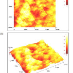 |
Figure 1: Two- (a) and three-dimensional (b) AFM images of CuS thin films deposited at pH 1 Click here to View figure |
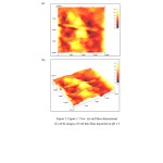 |
Figure 2: Two- (a) and three-dimensional (b) AFM images of CuS thin films deposited at pH 1.5 Click here to View figure |
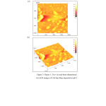 |
Figure 3: Two- (a) and three-dimensional (b) AFM images of CuS thin films deposited at pH 2 Click here to View figure |
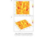 |
Figure 4: Two- (a) and three-dimensional (b) AFM images of CuS thin films deposited at pH 2.5 Click here to View figure |
In this work, I can find the film thickness using the AFM images. The results are presented in Table 1. It was observed that the thickness of the film was controlled by the pH adjustment. The thickness of the film was increased with increase in the pH of chemical bath up to 2. For further increase in pH, the film thickness was reduced.
Table 1: Thickness variation versus pH solution of the copper sulphide thin films
| pH | Thickness (nm) |
| 1 | 5.8 |
| 1.5 | 19.9 |
| 2 | 685.9 |
| 2.5 | 11.2 |
The surface roughness of the thin films was studied with AFM technique. Root mean square (RMS) roughness is defined as the standard deviation of the surface height profile
from the average height, is the most commonly reported measurement of surface roughness32. The surface roughness values of 0.80, 2.18, 47.02 and 0.78 nm have been observed for samples prepared at pH 1, 1.5, 2 and 2.5, respectively (Table 2). The surface roughness is unavoidable since grains were grown with different sizes and spherical in shapes.
Table 2: Surface roughness variation versus pH solution of the copper sulphide thin films
| pH | RMS (nm) |
| 1 | 0.80 |
| 1.5 | 2.18 |
| 2 | 47.02 |
| 2.5 | 0.78 |
Conclusions
Chemical bath deposited copper sulfide thin films were prepared in an aqueous solution by using controlled pH value (in the range of 1 to 2.5). Experiment findings show that smooth and smaller grain sizes of films were obtained in pH 1. Atomic force microscopy images showed that the film thickness in a range of 5.8 to 685.9 nm in various pH solutions.
Acknowledgement
INTI INTERNATIONAL UNIVERSITY is gratefully acknowledged for the financial support of this work.
References
- Marwa, F.; Shaimaa, E.; Siham, M.; Abd, E.B.K. Int. J. Electrochem. Sci., 2015, 10, 6030-6043.
- Kassim, A.; Ho, S.M.; Tan, W.T.; Saravanan, N. Orient. J. Chem., 2010, 26, 389-394.
- Lisco, F.; Kaminski, P.M.; Abbas, A.; Bass, K.; Bowers, J.W.; Claudio, G.; Losurdo, M.; Walls, J.M. Thin Solid Films, 2015, 582, 323-327.
CrossRef - Anuar, K.; Jelas, M.; Rosli, M.Y.; Tan, W.T.; Abdul, H.A.; Ho, S.M.; Saravanan, N. Kuwait J. Sci. Eng., 2010, 37, 63-73.
- Khomane, A.S. Optik, 2013, 124, 2432-2435.
CrossRef - Anuar, K.; Ho, S.M.; Atan, S.; Saravanan, N. Stud. UBB. Chem., 2010, 55, 5-11.
- Taisuke, I.; Shizutoshi, A. Thin Solid Films, 2012, 520, 7076-7082.
CrossRef - Anuar, K.; Ho, S.M.; Atan, S.; Haron, M.J. Res. J. Chem. Environ., 2011, 15, 45-48.
- Mane, R.M.; Ghanwat, V.B.; Kondalkar, V.V.; Khot, K.V.; Mane, S.R.; Patil, P.S.; Bhosale, P.N. Proc. Mater. Sci., 2014, 6, 1285-1291.
CrossRef - Ho, S.M. Oriental J. Chem., 2014, 30, 1009-1012.
- Harizi, A.; Sinaoui, A.; Akkari, F.C.; Kanzari, M. Mater. Sci. Semicond. Process, 2016, 41, 450-456.
CrossRef - Anuar, K.; Ho, S.M.; Atan, S.; Jelas, H.; Saravanan, N. Oriental J. Chem., 2011, 27, 1375-1381.
- Yeh, L.Y.; Cheng, K.W. J. Power Sources, 2015, 275, 750-759.
CrossRef - Anuar, K.; Tan, W.T.; Ho, S.M.; Abdul, H.A.; Ahmad, H.J.; Saravanan, N. Kasetsart J. (Nat. Sci), 2010, 44, 446-453.
- Fekadu, G.H.; Francis, K.A.; Tizzau, A.; Isaac, N.; Mark, P.; Robert, K.N.; Francis, B. Mater. Lett., 2015, 155, 58-61.
CrossRef - Anuar, K.; Tan, W.T.; Jelas, M.; Ho, S.M.; Gwee, S.Y. Thammasat Int. J. Sc. Tech., 2010, 15, 62-69.
- Rana, T.R.; Shinde, N.M.; Kim, J. Mater. Lett., 2016, 162, 40-43.
CrossRef - Anuar, K.; Ho, S.M.; Abdul, H.A.; Noraini, K.; Saravanan, N. Digest J. Nanomater. Biostructures, 2010, 5, 975-980.
- Mahendran, C.; Suriyanarayanan, N. Optik, 2015, 126, 4237-4242.
CrossRef - Anuar, K.; Ho, S.M.; Tan, W.T.; Ho, S.M.; Saravanan, N. Asian J. Res. Chem., 2012, 5, 291-294.
- Asenjo, B.; Guilln, C.; Chaparro, A.M.; Saucedo, E.; Bermudez, V.; Lincot, D.; Herrero, J.; Gutirrez, M.T. J. Phys. Chem. Solids, 2010, 71, 1629-1633.
CrossRef - Kassim, A.; Ho, S.M.; Abdullah, A.H.; Nagalingam, S. Trans. C: Chem. Chem. Eng., 2010, 17, 139-143.
- Gopakumar, N.; Anjana, P.S.; Vidyadharan, P.K. J. Mater. Sci., 2010, 45, 6653-6656.
CrossRef - Guneri, E.; Ulutas, C.; Kirmizigul, F.; Altindemir G.; Gode F.; Gumus, C. Appl. Surf. Sci., 2010, 257, 1189-1195.
CrossRef - Kale, R.B.; Lokhande, C.D.; Mane, R.S.; Han, S.H. Appl. Surf. Sci., 2007, 253, 3109-3112.
CrossRef - Sonawane, P.S.; Wani, P.A.; Patil, L.A.; Seth, T. Mater. Chem. Phys., 2004, 84, 221-227.
CrossRef - Nascu, C.; Pop, I.; Ionescu, V.; Indrea, E.; Bratu, I. Mater. Lett., 1997, 32, 73-77.
CrossRef - Zhuge, F.W.; Li, X.M.; Gao, X.D.; Gan, X.Y.; Zhou, F.L. Mater. Lett., 2009, 63, 652-654.
CrossRef - Podder, J.; Kobayashi, R.; Ichimura, M. Thin Solid Films, 2005, 472, 71-75.
CrossRef - Anuar, K.; Zainal, Z.; Hussein, M.Z.; Saravanan, N.; Haslina, I. Sol. Energy Mater. Sol. Cells, 2002, 73, 351-365.
CrossRef - Gadave, K.M.; Lokhande, C.D. Thin Solid Films, 1993, 229, 1-4.
CrossRef - Jiang, T.; Hall, N.; Ho, A.; Morin, S. Thin Solid Films, 2005, 417, 76-85.
CrossRef

This work is licensed under a Creative Commons Attribution 4.0 International License.
![]()
A New Edition of Web of Science
Journal Impact Factor
2022: 0.5
Five Year: 0.8
Journal is Indexed in

Cabells Whitelist
![]()


