Semiconducting Nanostructures and Nanocomposites for the Recognition of Toxic Chemicals
Sadia Ameen1, M. Shaheer Akhtar2 and Hyung Shik Shin1
1Energy Materials & Surface Science Laboratory, Solar Energy Research Center, School of Chemical Engineering, Chonbuk National University, Jeonju, 561-756, Republic of Korea
2New& Renewable Energy Material Development Center (NewREC), Chonbuk National University, Jeonbuk, Republic of Korea
DOI : http://dx.doi.org/10.13005/ojc/290302
Article Received on :
Article Accepted on :
Article Published : 28 Oct 2013
Semiconducting metal oxide and conducting polymers based nano structures possess unique morphological, optical and structural properties for the important applications in emerging technologies. On the other hand, the semiconducting nano composites offer the possibilities to control the properties by varying the composition of the materials and the related parameters such as morphology and an interface. This article provides a condensed overview of metal oxide and conducting polymer based semiconducting nano structures and nano composites for the development of chemical sensors. This work is a comprehensive review of current research activities that concentrate on chemical sensors based on metal oxides and conducting polymers nanostructures like nanotubes, nanorods,nanotubes, nanosheetsand nanoballs. The experimental principle, design of sensing devices, sensing mechanism, and the significant sensing parameters are comprehensively discussed.
KEYWORDS:semiconducting;nano structures;nano composites;toxic chemicals
Download this article as:| Copy the following to cite this article: Ameen S, Akhtar M.S, Shin H. S. Semiconducting Nanostructures and Nanocomposites for the Recognition of Toxic Chemicals. Orient J Chem 2013;29(3) |
| Copy the following to cite this URL: Ameen S, Akhtar M.S, Shin H. S. Semiconducting Nanostructures and Nanocomposites for the Recognition of Toxic Chemicals. Orient J Chem 2013;29(3). Available from: http://www.orientjchem.org/?p=221 |
Introduction
Semiconductor nanomaterials have attracted significant attention in research and applications in areas including energy conversion, sensing, electronics, photonics, and biomedicine. The parameters such as size, shape, and surface characteristics of semiconducting nanomaterials are significant to control the properties for different applications. Withthe development of nanoscience and nanotechnology, one-dimensional (1D) semiconducting nanostructured materials including nanotubes, nanorods, nanosheets, nanoballs, and other nano-structured materials have been widely applied to fabricate a variety of chemosensors. The 1D nanomaterial provides unique physicaland chemical properties, large surface area/volume ratio,good conductivity, excellent electrocatalytic activity and high mechanical strength.1Forsome specific applications,it is highly desired to control and alter the properties of nanomaterials with greater flexibility and possibility and thus, nanocomposites are the best alternatives to serve these purposes.The nanocomposites generally contain more than one single component and therefore, it is a simple approach to achieve the properties which are different from those of single component nanomaterials.
Conducting polymers likepolypyrrole, polythiophene, polyindol, polyaniline and polyfuran families are known as p-type semiconductors with unique electronic properties, low energy optical transitions, low ionization potential and high electron affinity2 thus, widely used as sensitive materials for conductometric polymer sensors. The main advantages of conducting polymers are the possibilityof working at room temperatures and simplicity of technology that significantly simplifies design of conducting polymers based devices and allows using them in portable instruments. Conducting polymers could be easily synthesized through simple chemical or electrochemical processes and their conductivities could be altered by modifying the electronic structures through doping or de-doping procedures.3Therefore, conducting polymers could suitably work as an effective working electrode and might offer the fast response towards the detection of various harmful chemicals.
The sensor technology is popularly known for the detection of harmful chemicals. The sensitivity, selectivity, and stability are the most important aspect of investigation of a variety of sensors. Up to now, efforts have been made by controlling the sensors structures,4-5sensor fabrication techniques6-7and surface modification8-9to detect the toxic chemicals. Among several sensors like fluorescence based chemical sensors,10chemically modified electrode chemical sensors11and chemiluminescence based sensors,12the electrochemical method provides the advantages of high sensitivity, wide linear range, economical, rapid response, portability and ease of operating procedure.13-14However, the electrochemical method is still a challenge to enhance the electron transfer rate over the surface of working electrode for sensors. Therefore, the modifications of the electrodes with different inorganic and organic nanomaterials could be promising for the reliable and effective detection of harmful chemicals by electrochemical and current-voltage (I-V) characteristics.
In this review, we have briefly discussed the semiconducting metal oxides nanostructures like TiO2, ZnO, conducting polymers and its nanocomposites for the efficient detection of harmful and toxic chemicals. The chapter includes the brief literature surveys, properties and the latest research advancements/trends for the development of various metal oxides nanostructures, nanocomposites and conducting polymer based nanomaterials as efficient electrode for detecting harmful chemical through the effective electrochemical technique. The preparation methods, morphologies, the physical and chemical properties of metal oxides, nanocomposites and conducting polymers have shown the significant impacts on the optical, electrical, electronic properties of the nanomaterials, and their performances for detecting the harmful chemicals.
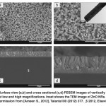 |
Fig. 1: Surface view (a,b) and cross sectional (c,d) FESEM images of vertically aligned ZnO NRs at low and high magnifications. Inset shows the TEM image of ZnO NRs. Reprinted with permission from [Ameen S., 2012], Talanta100 (2012) 377. Ⓒ 2012, Elsevier Ltd. Click here to View figure |
Semiconducting Metal oxide Nanostructures for Chemosensors
Modified Electrode of Vertically Aligned ZincOxide Nanorods for the Detection of Hydrazine Chemical Sensor
The inorganic metal oxide materials in nanoscale have recently received a great deal of interest owing to their unique structures, electrical, and catalytic properties.15-16Zinc oxide (ZnO) nanomaterials have been extensively explored as the most encouraging materials for many optical-electrical and the photovoltaic devices.17-19 The nanocrystalline ZnO20with wide band gap of ~3.37 eVexhibits high exciton, binding energy, low-cost synthesis, biocompatibility, better electrochemical activities, non-toxicity, chemical and photochemical stability and high-electron communication features.21-22Moreover, ZnO nanomaterials based electrodes have shown good electrochemical activities towards chemicals, biomolecules and gases owing to their high-electron transfer characteristics with high electrochemical and photochemical stability.23-24 Recently, one-dimensional (1D) ZnO nanostructures such as nanorods, nanobelts, nanowires and nanotubes have been studied for fabricating various electrochemical and photoelectrochemical devices due to their sufficiently high surface-to-volume ratio and good electrical characteristics.25-261D ZnO aligned nanostructures could be promising and effective electrodes for sensing applications towards the detection of various chemicals and biomaterials. So far, few literatures have reported on the electrochemical detection of hydrazine and its derivatives using ZnO nanostructures based modified electrodes.27-28Ni et al fabricated hierarchical micro/nanoarchitecture ZnO based electrodes for hydrazine sensing with the sensitivity of ~0.51μAμM-1cm-229.Fang et al demonstrated the utilization of ZnO nanoflowers modified electrode for the fabrication of hydrazine chemical sensor with the sensitivity of ~3.49 μA μM-1cm-2.30A. Umar et al reported the electrochemical sensor for the detection of hydrazine over the surface of gold electrode modified with ZnO nanorods.31Ameen et al32reported a simple and less expensive low temperature hydrothermal method for the synthesis of highly uniform and vertically aligned ZnO NRs on FTO glass substrates. The synthesized vertically aligned ZnO NRs electrodes were directly applied for the effective detection of hydrazine through simple current (I)-voltage (V) characteristics. The fabricated vertically aligned ZnO NRs thin film modified electrode showed the rapid detection of hydrazine and exhibited the high sensitivity of ~4.42446 x 10⁻⁵ A.mM-1.cm-2and detection limit of ~515.7 µM with correlation coefficient (R) of ~0.73297 and short response time (10 s).
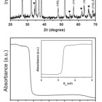 |
Fig. 2: XRD patterns (a) and UV-DRS spectrum (b) of vertically aligned ZnO NRs.Reprinted with permission from [Ameen S., 2012], Talanta 100 (2012) 377. Ⓒ 2012, Elsevier Ltd. Click here to View figure |
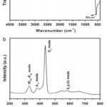 |
Fig. 3: FTIR (a) and Raman scattering (b) spectrum of vertically aligned ZnO NRs. Reprinted with permission from [Ameen S., 2012], Talanta 100 (2012) 377. Ⓒ 2012, Elsevier Ltd. Click here to View figure |
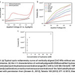 |
Fig. 4: (a) Typical cyclo voltammetry curve of vertically aligned ZnO NRs without and with hydrazine, (b) the I–V characteristics of vertically aligned ZnONRs modified hydrazine chemical sensor in hydrazinec on centration range of 0.3 mM to0.03Min10mlof0.1MPBS solution and (c)calibration curve of current versus concentrations of the fabricated hydrazine sensor. Reprinted with permission from [Ameen S., 2012], Talanta 100 (2012) 377. Ⓒ 2012, Elsevier Ltd. Click here to View figure |
The highly dense ZnO NRs could be seen in the surface view image at low magnification (Fig. 1(a)). The high magnification image, as shown in Fig. 1(b), displays the typical hexagonal structure of ZnO NRs with the average diameter of ~200-300 nm. The cross-sectional view (Fig. 1(c,d)) reveals the densely vertically aligned ZnO NRs on FTO substrates. The ZnO NRs possesses the average diameter of ~200-300 nm and length of ~3-5 µm. It clearly suggests that the thin layer of ZnO seed significantly results the uniform vertically aligned ZnO NRs on the FTO substrate with the average thickness of ~5 µm. In support, the vertically aligned ZnO NRs are further characterized by the TEM analysis, as shown in the inset of Fig. 1(b). The typical ZnO hexagonal structure with the average diameter of ~200-300 nm is seen, which is much consistent with the FESEM results.
Fig. 2(a) shows the XRD patterns of vertically aligned ZnO NRs deposited on the FTO substrate. The grown ZnO NRs exhibit the crystalline peaks of ZnO at 32.2o, 34.8o, 36.6o, 48.1o, 57.3o, 63.4o and 68.6o which match well with JCPDS No. 36-1451.33These patterns are attributed to the typical wurtzite structure of ZnO crystals. However, the diffraction peaks at 26.8o, 34.2o, 51.9o, 55o, 62oand 66.2oare associated with of the FTO substrate.34Noticeably, the diffraction peak (101) indicates the preferential orientation due to the vertical growth of NRs on the FTO substrate.35Fig. 2(b) shows the UV-DRS spectra and derived band energy plot of vertically aligned ZnO NRs is shown as inset of Fig. 2(b). The ZnO NR obtains the broad intense absorption edge from ∼400 nm to lower wavelengths region, originating from a charge-transfer process from the valence band to conduction band of ZnO.36The band gap of vertically aligned ZnO NRs is calculated as ~3.29eV which is very close to the band gap of bulk ZnO nanomaterials.37
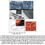 |
Fig. 5: FESEM images of TiO2 NT arrays at low (a) and high (b) magnification.Inset of (a) shows cross section image of TiO2 NT arrays, TEM image(c), and HRTEM image (d) of TiO2 NT arrays. Inset of (c) shows SAED patternsof TiO2 NT arrays, (e) Raman spectrum and inset of (e) shows the correspondingRaman mapping images in 390-460 cm-1, and (f) thecorresponding Raman mapping images 550–650 cm-1 of TiO2NT arrays.Reprinted with permission from [Ameen S., 2013], Appl. Phys. Lett.103 (2013) 061602.Ⓒ2013,AIP Publishing LLC. Click here to View figure |
The structural properties of vertically aligned ZnO NRs are studied by analyzing the FTIR spectrum, as shown in Fig. 3(a). A very intense IR band at ~554 cm-1 is ascribed to the typical Zn–O group of bulk ZnO,38suggesting that the synthesized ZnO NRs possess pure Zn–O groups. The appearance of IR peaks at ~3404 and ~1560 cm-1 are originated from OH stretching mode and water scissoring vibration or the carboxylate anion asymmetrical stretching respectively.39Moreover, the IR band at ~1087 and ~878cm-1 are assigned to υ1 stretching frequency and the bending vibration of nitrate respectively. The investigation of the structural disorder and the defects of the vertically aligned ZnO NRs are elucidated by the Raman scattering spectroscopy, as shown in Fig. 3(b). The presence of strong peak at ~437cm-1 is ascribed to E2 mode of ZnO crystal which matches with Raman peak of bulk ZnO crystals.40The other two weak peaks at ~331.2 and ~382.1cm-1 are due to the second order Raman spectrum arising from zone-boundary phonons 3E2H–E2L for wurtzite hexagonal ZnO single crystals and A1T modes respectively. However, the broader peak at ~586cm-1 corresponds to E1 (LO) mode of ZnO associated with oxygen deficiency in ZnO nanomaterials. It is known that the appearance of intense E2 mode is represented to the better optical and crystalline properties of ZnO nanomaterials.41In our case, the synthesized vertically aligned ZnO NRs possess the high crystallinity of ZnO crystals with less oxygen vacancies.
 |
Fig. 6: (a) Typical amperometric plot and (b) linear plot of current versus concentration of phenyl hydrazine of TiO2 NT arrays based chemical sensor. (c) The I-V characteristics and (d) the calibration curve of current versus phenyl hydrazine concentration of TiO2 NT arrays electrode based chemical sensor at different phenyl hydrazine concentrations (0.25 lM–0.10mM) in 10ml of 0.1M PBS, and (e) schematic illustration of proposed mechanism of phenyl hydrazine chemical sensors over the surface of TiO2 NT arrays based electrode.Reprinted with permission from [Ameen S., 2013], Appl. Phys. Lett. 103 (2013) 061602.Ⓒ2013, AIP Publishing LLC. Click here to View figure |
The electrochemical response of vertically aligned ZnO NRs electrode is studied to investigate the electrocatalytic activity of vertically aligned ZnO NRs towards hydrazine. Fig. 4(a) shows the typical cyclic voltammogram (CV) of vertically aligned ZnO NRs electrode without and with hydrazine in 0.1 M phosphate buffer (pH=7.0) at the scan rate of 100 mV/s. The sensing response is generally detected by oxidation process of hydrazine. The CV with vertically aligned ZnO NRs electrode displays that the oxidation process begins from ~-0.38V and achieves the maximum anodic current of~0.124mA at -0.109 V.Only the anodic current occurs due to the irreversible electrochemical response towards hydrazine. It is noticed that the anodic current of electrochemical system has significantly increased with the addition of hydrazine concentrations in PBS, while a negligible or very low current is observed without hydrazine. The high height and current of anodic peak are usually attributed to a faster electron-transfer reaction in the electrochemical system via high electrocatalytic behavior of electrode.42Herein, the vertically aligned ZnO NRs electrode exhibits the increased current with high height of anodic peak in presence of hydrazine, confirming the involvement of high electron transfer process via high electrocatalytic activity of electrode. The current (I)–voltage (V) characteristics have been measured for the fabricated hydrazine sensor with vertically aligned ZnO NRs thin film as working electrode to evaluate the sensing properties. The fabricated hydrazine chemical sensor based on vertically aligned ZnO NRs thin film as working electrode is illustrated in Fig. 4(b). A series of I-V characteristics has been tested with various concentrations of hydrazine ranging from 0.3µM–0.03M in 0.1 M PBS for detecting the sensitivity of the fabricated chemical sensor. From Fig. 4(b), the presence of hydrazine in the fabricated chemical sensor shows an immediate increase in the current (~4.6 x 10⁻⁶ A) as compared to without hydrazine based chemical sensor (~9.3 x 10⁻⁷ A). The substantial increment in current clearly reveals that a good sensing response towards the detection of hydrazine is associated with the vertically aligned ZnO electrode which might result from its better electrocatalytic activity and fast electron exchange. Moreover, a series of the I-V characteristics is shown in Fig.4(b) which elucidates the sensing properties of the fabricated hydrazine chemical sensor. With the increase of hydrazine concentrations (0.3µM–0.03M), the current has continuously increased, which might originate by the generation of large number of ions and the increase of ionic strength of the solution with the addition of different concentration of hydrazine.The calibration curve of current versus concentration is plotted to analyze the sensitivity of the fabricated hydrazine sensor, as shown in Fig. 4(c). The current increases with the increase of hydrazine concentrationsupto~3 mM and then reaches to a saturation level as visible in the calibrated plot. This phenomenon comes out due to the unavailability of free active sites over vertically aligned ZnO NRs electrode for hydrazine adsorption at the higher concentration of hydrazine (>0.03 M).The calibration curve is plotted to estimate the sensitivity of hydrazine by taking the slope and divided by an active area of the electrode (0.5 cm2). The vertically aligned ZnO NRs electrode based hydrazine chemical sensor shows high and the reproducible sensitivity of ~4.42446 x 10⁻⁵ A.mM-1.cm-2with a correlation coefficient (R) of ~0.73297, the detection limit of ~ 515.7 µM and a short response time (10 s).The fabricated hydrazine sensor shows a good linearity in the range of 0.3µM-0.3mM. The stability of hydrazine chemical sensor was determined by measuring the I-V characteristics for three consecutive weeks. The fabricated hydrazine sensor did not show any significant decrease in the sensing parameters or properties, confirming the long term stability of the fabricated hydrazine sensor based on vertically aligned ZnO NRs electrode. Enhancement of the sensing properties might due to the unique vertically aligned morphology of ZnO NRs containing subtle optical, electronic behaviors and strong electrocatalytic activity. Therefore, the vertically aligned ZnO NRs electrode is a promising working electrode for the effective detection of hydrazine.
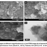 |
Fig. 7: FESEM images at different magnifications (a–c) and TEM image (d) of layered PANI nanosheets. Reprinted with permission from [SeoH.K., 2013], Talanta,104 (2013) 219. Ⓒ 2013, Elsevier Ltd. Click here to View figure |
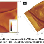 |
Fig. 8: Topographic (a) and three dimensional (b) AFM images of layered PANI nanosheets.Reprinted with permission from [Seo H.K., 2013], Talanta, 104 (2013) 219. Ⓒ 2013, Elsevier Ltd. Click here to View figure |
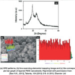 |
Fig. 9:(a) XRD patterns, (b) line scanning elemental mapping image and (c) the corresponding pie bar graph of layered PANI nanosheets. Reprinted with permission from [Seo H.K., 2013], Talanta, 104 (2013) 219. Ⓒ 2013, Elsevier Ltd. Click here to View figure |
Prospective Electrode of TiO2 Nanotube Arrays for the of Sensing of Phenyl Hydrazine
The nanostructures of titania (TiO2) are one of most versatile metaloxides, exhibiting exotic inert surface and the optical properties. The tailoring of multidimensional TiO2 nanostructures to one dimensional (1D) is playing a significant role for determining the physiological and electrical properties. Among various1D TiO2 nanostructures, TiO2 NTs generally exhibits the large surface area43outstanding charge transport properties,44excellent electronic, mechanical, and chemical stability properties.45In particular, TiO2 NTs with highly uniform morphology and unique-orientated growth properties are promising forthe applications in gas sensors, biosensors,46dye sensitized solar cells,47hydrogen generation,48and supercapacitors. Recently, TiO2 nanostructures with high surface area are extensively utilized forthe detection of harmful chemicals through sensing. Kwonet al. studied the enhanced ethanol sensing properties over thesurface of TiO2 NTs electrode based sensors.49 Chen et al. fabricated a room-temperature hydrogen sensor with TiO2 NT arrays based electrode.50Ameen et al51synthesized TiO2 NT arrays on Ti foil substrate by simple electrochemical anodicoxidation and utilized as the working electrode for the fabrication of a highly sensitive, reliable, and reproducible chemical sensor for the detection of harmful phenyl hydrazine chemical. The fabricated phenyl hydrazine sensor showed high sensitivity of ~40.9 µAmM-1cm-2 and the detection limit of~0.22 µM. The good compatibility, high uniformity, and the large surface area have made TiO2 NT arrays electrode as promising chemosensor for the rapid, sensitive, andselective detection of phenyl hydrazine chemical.
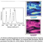 |
Fig. 10: Raman scattering spectrum (a) and its corresponding Raman mapping in 1300-1400cm-1 (b) and in 1550-1600cm-1 (c) of layered PANI nanosheets. Reprinted with permission from [Seo H.K., 2013], Talanta, 104 (2013) 219. Ⓒ 2013, Elsevier Ltd. Click here to View figure |
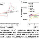 |
Fig. 11: (a) Typical cyclo voltammetry curve of fabricated phenol chemical sensor based layered PANI nanosheets electrode without and with phenol (20 mM) in10ml of 0.1M PBS solution and (b) CV sweep curves in phenol concentrations of 20 mM–0.32 mM in 10ml of 0.1M PBS solution.Reprinted with permission from [Seo H.K., 2013], Talanta, 104 (2013) 219. Ⓒ 2013, Elsevier Ltd. Click here to View figure |
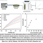 |
Fig. 12: (a) Schematic illustration of the fabricated phenol chemical sensor, (b) I–V characteristics of layered PANI nanosheets based phenol chemical sensor at different phenol concentrations (20 mM–0.32mM) in10ml of 0.1 MPBS and (c) the calibration curve of current versus phenol concentration of the fabricated chemical sensor.Reprinted with permission from [Seo H.K., 2013], Talanta, 104 (2013) 219. Ⓒ 2013, Elsevier Ltd. Click here to View figure |
The grown TiO2 on Ti substrate displays highly ordered and self-assembled NT arrays, as shown in Fig. 5(a). At high magnification (Fig. 5(b)), a uniform and closely packed TiO2 NT arrays are seen. Moreover, the grown TiO2 NT arrays present distinguishable diameter distribution. The average diameter and wall thickness of TiO2 NT arrays are observed as 100±20 nm and 20±5 nm, respectively. The inset of Fig. 5(a) depicts the cross-sectional FESEM image of grownTiO2 NT arrays which exhibits the average length of~15µm. A hollow tubular morphology could be seen in the TEM image of grown TiO2 NT arrays (Fig. 5(c)),which is consistent with the FESEM results. The TiO2 NT arrays exhibit the average diameter and wall thickness of100±20 nm and 20±5 nm, respectively. The SAED pattern of TiO2 NT arrays (inset of Fig. 5(c)) shows polycrystallinephases in the anatase TiO2. The HRTEM image of TiO2 NTarrays (Fig. 5(d)) shows well-resolved lattice fringes of crystallineTiO2 NT arrays with plane spacing of ~0.35 nm,which corresponds to anataseTiO2 (101). These observations considerably deduce the good crystallinity of grown TiO2NT arrays. The phase composition and structural properties of TiO2 NT arrays are investigated by Raman scattering spectroscopy and the corresponding mapping, as shown in Figs. 5(e) and 5(f). The grown TiO2 NT arrays obtain three active Raman modes at~396.1, ~518.2, and ~637.4 cm-1 which correspond to the active Raman modes of anatase phase with symmetries ofB1g(1), (B1g(2) + Ag(1)), and Eg3, respectively, and match with the Raman modes of anataseTiO2.52-53Consequently,Raman spectrum does not exhibit any Raman mode at~445 cm-1, indicating that no rutile phase exits in the grownTiO2 NT arrays. The inset of Fig. 5(e) shows the Raman mapping in the range of ~390–460 cm-1 and reveals the largerdark part which corresponds to the peak at ~396.1 cm-1whereas Fig. 5(f) shows the Raman mapping in the range of~550–650 cm-1 which exhibits highly uniform surface, suggestingthat the grown TiO2 NT arrays are in good quality ofanataseTiO2 phase.
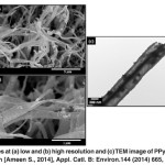 |
Fig. 13: FESEM images at (a) low and (b) high resolution and (c) TEM image of PPynanobelts. Reprinted with permission from [Ameen S., 2014], Appl. Catl. B: Environ.144 (2014) 665,Ⓒ 2014, Elsevier Ltd. Click here to View figure |
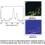 |
Fig. 14: (a) Raman spectrum and (b) corresponding Raman mapping images in 950-1050 cm−1and (c) 1550-1600 cm−1of PPynanobelts Appl. Catl. B: Environ. 144 (2014) 665, Ⓒ 2014, Elsevier Ltd. Click here to View figure |
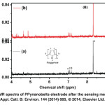 |
Fig. 15:1H NMR spectra of PPynanobelts electrode after the sensing measurements.Appl. Catl. B: Environ. 144 (2014) 665, Ⓒ 2014, Elsevier Ltd. Click here to View figure |
The steady state current-time or amperometric responses of the system are measured to further investigate the electrocatalytic behavior of TiO2 NT arrays electrode towards phenyl hydrazine chemical at low concentration. The steady-state current is achieved in a PBS of pH7 withthe successive addition of phenyl hydrazine (0-0.3 µM)using the peristaltic pump with respect to Ag/AgCl referenc eelectrode. The typical amperometric plot is shown inFig. 6(a). In the beginning, the electrochemical experiment is performed in PBS without phenyl hydrazine for stabilizing the background current. The successive addition of phenyl hydrazine has shown the linear increase in current, exhibiting a linear relationship between the current and phenyl hydrazine concentrations. Fig. 6(b) depicts the linear plot of current versusconcentration of phenyl hydrazine for TiO2 NT arrays electrode which again confirm the linear relationshipbetween current and concentration of phenyl hydrazine. These observations infer that the TiO2 NT arrays electrode is highly effective catalyst to detect the sensing response ofphenyl hydrazine at very low concentration which might attribute to the good electrocatalytic, and direct electrontransfer or fast electron exchange behavior of TiO2 NTarrays.The current (I)-voltage (V) characteristics are measuredfor evaluating the sensing properties (sensitivity,detection limit, and correlation coefficient) of the fabricated phenyl hydrazine chemical sensor over TiO2 NT arrayselectrode. The current response is measured from0.0–2.5V, and the time delaying and response times are 1.0 and 10 s, respectively. From Fig. 6(c), the current has continuously increased with the increase of thephenyl hydrazine concentrations from 0.25µM–0.10 mM, suggesting the good sensing response towards phenyl hydrazine chemical by TiO2 NT arrays electrode. The enhancement in current might due to the better electrocatalytic behavior, generation of large number of ions, and the increase of ionic strength of the solution with the addition of phenyl hydrazine. The sensing parameters such as sensitivity, detection limit, and correlation coefficient are calculated by a calibration curve of current versusphenyl hydrazine concentration of the fabricated phenyl hydrazine chemical sensor. Fig. 6(d) presents the plot of calibration current versus phenyl hydrazine concentration which reveals that the current increases linearly up to the phenyl hydrazine concentration of ~1µM and afterwards achieve a saturation level in the calibrated plot. The saturation point occurs due to the less availability of free active sites on the surface of TiO2 NT arrays electrode for phenylhydrazine chemical at higher concentration (>10 µM) inPBS. The fabricated phenyl hydrazine chemical sensor based on TiO2 NT arrays electrode exhibits significantly high and reproducible sensitivity of ~40.9 µAmM-1cm-2and the detection limit of ~0.22µM with correlation coefficient(R) of ~0.98601 and short response time of 10 s. Importantly, the fabricated phenyl hydrazine chemical sensor based on TiO2 NT arrays electrode displays a good linearity in the range of 0.25 µM-1µM. The phenyl hydrazine sensing mechanism over the surface of TiO2 NT arrays electrode is explained by using the surface-depletionmodel.54 Fig. 6(e) shows the illustration of sensing response of phenyl hydrazine chemical over the surface of TiO2 NTarrays electrode. Primarily, the phenyl hydrazine is chemisorbed on the surface of TiO2 NT arrays. TiO2 NT arrays interact easily with atmospheric oxygen by transferring electrons from the conduction band to the adsorbed oxygenatoms and presents in the form of O–, O2–, etc.,54 as shown in Fig. 6(e). Second, these oxygenated species interact with phenyl hydrazine and oxidizes phenyl hydrazine into less harmful diazenyl benzene on the surface of TiO2 NT arrays.Thus,TiO2 NT arrays electrode provides suitable surface for the oxidation of phenyl hydrazine and determines the sensing responses by increases the current values. The reusability and reproducibility of the fabricated phenyl hydrazinechemical sensor based on TiO2 NT arrays electrode were elucidated by measuring the sensing responses with the I-Vcharacteristics for three consecutive weeks. The sensing parameters or properties showed the negligible drops in the fabricated phenyl hydrazine chemical sensor based on TiO2NT arrays electrode, which deduces the long term stability of the fabricated phenyl hydrazine chemical sensor. Thus, TiO2 NT arrays with anatase phase and good crystal quality are promising and effective working electrode for the detection of phenyl hydrazine chemical or other hazardous chemicals.
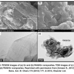 |
Fig. 16: FESEM images of (a) Gr and (b) PANI/Gr composites. TEM images of (c) Gr and (d) PANI/Gr composites. Reprinted with permission from [Ameen S., 2012], Sens. Act. B: Chem.173 (2012) 177,Ⓒ 2012, Elsevier Ltd. Click here to View figure |
Conducting Polymers based Nanostructures for Chemosensors
Conducting polymers are known as p-type semiconductors and offer unique electronic properties owing to their good electrical conductivity, low energy optical transitions, low ionization potential and high electron affinity.55These polymers could be easily synthesized through simple chemical or electrochemical processes and their conductivities could be altered by modifying the electronic structures through doping or de-doping procedures.56The good selectivity, wide linear range, rapid response, portability and the room temperature working abilities are the basic requirements for the efficient working of chemical sensors.57The conducting polymers are widely used as sensitive materials for chemosensors as they are effective working electrode and might offer the fast response towards the detection of various harmful chemicals.58
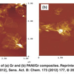 |
Fig. 17: AFM images of (a) Gr and (b) PANI/Gr composites. Reprinted with permission from [Ameen S., 2012], Sens. Act. B: Chem. 173 (2012) 177, Ⓒ 2012, Elsevier Ltd. Click here to View figure |
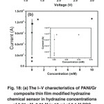 |
Fig. 18: (a) The I–V characteristics of PANI/Gr composite thin film modified hydrazine chemical sensor in hydrazine concentrations of 0.01 µM–0.01 M in 10 ml of 0.1 M PBS solution and (b) calibration curve of current versus concentrations of the fabricated hydrazine sensor. Inset (a) shows typical cyclovoltametry curve for PANI/Gr modified electrode without and with hydrazine, and inset (b) the calibration curve of current in the lower concentrations region.Reprinted with permission from [Ameen S., 2012], Sens. Act. B: Chem. 173 (2012) 177, Ⓒ 2012, Elsevier Ltd. Click here to View figure |
The Efficient Electrode of Layered Polyaniline (PANI)Nanosheetsfor the Detection of Hazardous Phenol Chemical
A unique organic p-type semiconductor polymer, polyaniline (PANI) is highly searched polymer due to its unique acid-base chemistry, stable electrical conduction, high-environmental stability and ease of fabrication.59Importantly, PANI possesses the typical conjugated bonds in the polymer skeleton which could be responsible for the charge conduction due to the generation of polarons or bipolarons.60The variable conductivity makes PANI as promising material for the specific application of electronics, optoelectronic, electrochemical, electrochromic, photovoltaic and sensing devices.61Moreover, the presence of the reactive NH- groups in the polymer chain (PANI), positioned on either side by phenylene rings imparts the chemical flexibility to the system and improves the processibility to a large extent. PANI nanomaterial shows the versatility of nanostructures in the form of nanofibers, nanorods, nanowires and nanoflakes with high surface/volume ratio and low diffusional resistance.62Various PANI nanostructures display the improved optical, structural, electronic and electrical properties which might act as useful candidate for the application in electrochemical, electrochromic, biosensors and chemical sensors devices.63-64 Recently, PANI nanomaterials have gained a great attention in the field of sensors including gas sensor, biosensor and chemical sensors.65 In context of PANI based sensors, A. L. Kukla et al prepared PANI thin films for detecting ammonia.66Y. Bo et al explained the electrochemical DNA biosensor by PANI nanowires modified graphene electrode.67Recently, P. Kunzo et al fabricated the hydrogen sensor based on unique oxygen plasma treated PANI thin film.An amperometric phenol biosensor based on PANI electrode was studied in the aspects of optical and electrochemical properties.68J. Zhang et al designed the composite electrode of PANI-ionic liquid-carbon nanofiber for the fabrication of highly sensitive amperometric biosensors towards phenols.69Ameen et al reported the layered PANI nanosheets based electrodes as an effective chemical sensor towards the efficient detection of phenol.70The fabricated phenol sensor based on layered PANI nanosheets exhibited a high sensitivity of ~1485.3 µA.mM-1.cm-2and very low detection limit of ~4.43 µM with correlation coefficient (R) of ~0.9981 and short response time (10 s).
Fig.7 shows the FESEM and TEM images of layered PANI nanosheets. At low resolution (Fig. 7(a-b)), the synthesized PANI displays the uniform and compact layered sheets like morphology. The layered PANI nanosheets exhibit the average thickness of several hundred nanometers, as shown in Fig. 7(c). The morphology of synthesized PANI is further characterized by TEM analysis, as depicted in Fig. 7(d). The layered morphology of PANI nanosheets is clearly visible which is similar to the FESEM results. There is no deformation of the morphology of layered PANI nanosheets under the high electron beam of TEM, suggesting the stability of the synthesized layered PANI nanosheets.
Fig.8 shows the topographic and three dimensional (3D) AFM images of layered PANI nanosheets. The layered morphology of synthesized PANI is visibly recorded in the topographic mode, as shown in Fig. 8(a). The 3D AFM image (Fig. 8(b)) has confirmed the same layered morphology, as detected in the topographic mode. The roughness of layered PANI nanosheets is estimated from AFM images by taking the value of the root mean roughness (Rrms). The layered PANI nanosheets exhibit relatively the high roughness of ~52.3 nm. It is known that the electrode materials with large roughness factor display higher electrochemical behavior or the electrocatalytic activity.The high roughness of layered PANI nanosheets might improve the electrochemical behavior towards the detection of phenol.
Fig. 9(a) shows the X-rays diffraction (XRD) patterns of layered PANI nanosheets. Typically, two diffraction peaks at 19.3o and 25.1o are recorded, corresponding to the periodicity parallel and perpendicular to the polymer chain, respectively. These peaks are also assigned to emeraldine structure of PANI. The recorded XRD patterns are similar to PANI sheets or matrix.71 The element composition of the layered PANI nanosheets is analyzed by taking the line scan element mapping through EDS. Fig. 9(b, c) shows the line scan element mapping image and pie profile of the elements. The C and N elements are majorly distributed in the line scan mapping however, the traces of Cl and S elements are also detected, as seen in the corresponding pie bar graph shown in Fig. 9(c). The uniform distribution of C and N elements confirm the formation of layered PANI nanosheets.
The structural properties are further characterized by the Raman scattering spectroscopy, as shown in Fig. 10(a). The Raman band at ~1169 cm−1 is attributed to the C–C stretching/C–H in plane bending of the synthesized layered PANI nanosheets.72 The observation of Raman band at ~1371 cm-1 is assigned to the presence of C~N•+ (where ‘~’ denotes an intermediate bond between a single and a double) stretching mode of the delocalized polaronic charge carriers in PANI.73 Moreover, the Raman bands at ~1494 and ~1587 cm−1 is associated to N–H bending/C–H bending of benzenoid and C=C (Quinoid)/C–C (benzenoid) stretching respectively.74 The corresponding Raman mapping images in the two ranges of ~1300-1400 cm-1 and ~1550 – 1600 cm-1 are depicted in Fig. 10(b-c). The Raman mapping in the range of 1300-1400 cm-1 (Fig. 10(b)) shows the scatteredlight blue color on the major blue area of mapping, which might present the C~N•+ stretching modes (Raman shift at ~1371 cm−1)of delocalized polaronic charge carriers in PANI backbone.However, uniform distribution of the C=C (Quinoid)/C–C (benzenoid) stretching in layered PANI nanosheets are observed in the range of 1550-1600 cm-1,as shown in Fig. 10(c). Thus, the uniformly distributed C=C/C-C bonding along with C~N•+bonding in Raman mapping confirms the formation of high quality of layered PANI nanosheets.
The electrocatalytic activity of layered PANI nanosheets electrode towards the detection of phenol is examined by the cyclicvoltametry (CV) analysis. Fig. 11 shows the typical CV of layered PANI nanosheets electrode without and with a series of phenol concentrations (20 µM-0.32 mM) in 0.1 M phosphate buffer (pH=7.0) at the scan rate of 100 mVs-1. The layered PANI nanosheets electrode shows the relatively low redox current in the absence of phenol, as shown in Fig. 7(a). Importantly, the prominent oxidation peak with the maximum anodic current of ~1.1 x 10⁻⁴ A at ~0.37 V is obtained with the addition of lowest phenol concentration (20 µM), indicating the significant sensing response and high electrocatalytic activity over the surface of layered PANI nanosheets. The weak reduction peak with low cathodic current of -4.67 x 10⁻⁵ A is also observed in the CV curve. The electrochemical behavior with prominent oxidation peak along with weak reduction peak is quite similar to the reported literatures75and thus, the following reaction could be proposed for phenol. A series of CVplotshave been carried out with various phenol concentrations ranging from 20 µM – 0.32 mM in 0.1 M PBS to further examine the electrochemical properties of layered PANI nanosheets electrode. Fig. 11(b) shows the typical quasi-reversible redox peaks to the electrochemical reaction of layered PANI nanosheets electrode towards the phenol chemical in PBS. The oxidation peak is gradually increased with the increase of phenol concentration from 20 µM – 0.32 mM. It is reported that the high height of oxidation peak and the high anodic current are referred to the faster electron-transfer reaction in the electrochemical system via high electrocatalytic behavior of the working electrode.76The highest anodic current is obtained at the highest concentration of phenol (0.32 mM), which is about 2 times larger than the lowest phenol concentration 20 µM. The considerable increased of the anodic current demonstrates that the electrochemical activity of layered PANI nanosheetselectrode is remarkably promoted for the detection of phenol chemical and thus, confirms the involvement of high electrons transfer process via high electrocatalytic activity of the electrode.
The fabricated phenol chemical sensor is illustrated in Fig. 12(a), which is comprised of layered PANI nanosheets electrode as working electrode and Pt wire as cathode electrode in PBS. The measurement of current(I) – voltage(V) characteristics (Fig. 12(b)) is performed for evaluating the sensing properties such as sensitivity, detection limit and correlation coefficient of layered PANI nanosheets electrode towards phenol chemical. After the addition of phenol (20µM), the sudden increase in the current of ~67.3 µA is observed by the fabricated phenol chemical sensor however, a low current (~11.1 µA) is recorded without phenol based chemical sensor. A series of the I-V characteristics have been established to elucidate the sensing parameters of the fabricated phenol chemical sensor with layered PANI nanosheets electrode, as shown in Fig. 12(b). It is seen that thecurrent has continuously increased with the increase of the phenol concentrations (~20 µM – 0.32 mM), suggesting the good sensing response toward the phenol chemical by the layered PANI nanosheets electrode based phenol chemical sensor. This phenomenon might originate by the generation of large number of ions and the increase of ionic strength of the solution with the addition of different concentration of phenol. A calibration curve of current versus phenol concentration (Fig. 12(c)) is plotted to calculate the sensitivity of the fabricated phenolchemical sensor. The calibrated current linearly increases up to the increase of the phenol concentrations ~80 µMand then attains a saturation level in the calibrated plot. The occurrence of the saturation point might due to the unavailability of free active sites over the layered PANI nanosheetselectrode for phenol adsorption at higher concentration(>80 µM).The fabricated phenol chemical sensor with layered PANI nanosheets electrode achieves high, and the reproducible sensitivity of ~1485.3 µA.mM-1.cm-2 and the detection limit of ~4.43 µM with correlation coefficient (R) of ~0.9981 and short response time (10 s). A good linearity in the range of 20 µM – 80 µM is detected by the fabricated phenol chemical sensor with layered PANI nanosheetselectrode. For reproducibility and the stability of fabricated phenol chemical sensor,the sensing response by the I-V characteristics is measured for three consecutive weeks. It is found that the fabricated phenol chemical sensor did not show any significant decrease in the sensing parameters or properties, which deduces the long term stability of the fabricated phenol sensor based on layered PANI nanosheets electrode. Thus, the unique layered morphology of PANI nanosheets is promising and effective as working electrode for the detection of phenol chemical.
PolypyrroleNanobelts as Prospective Electrode for the Direct Detection of Aliphatic Alcohols
Polypyrrole (PPy), a conducting polymer, is much explored material because it shows high electrical conductivity, high stability in air and aqueous media and thus, an extremely useful material for actuators, electric devices and for the efficient detection of the harmful chemicals.77-78Few literatures are reported on the sensor performances of PPy nanostructure based electrodes for the detection of aliphatic alcoholsS. J. Hong et al studied nitro vinyl substituted PPy as a unique reaction-based chemosensor for cyanide anion.79C.W. Lin et al. prepared the composite electrode of PPy-poly vinyl alcohol (PVA) by electrochemical method for the detection of methanol and ethanol vapor.80-81L. Jiang et al. prepared the composite films of PPy-PVA by in situ vapor state polymerization method and demonstrated the methanol sensing behavior based on the thickness of PPy-PVA film electrodes.82Recently, M. Babaei et al. determined the residual methanol content in the biodiesel samples by developing new PPy-ClO4 electrodes via electrode position on interdigital electrodes.83The roughness and morphology of the PPy greatly influence the responses for the detection of harmful chemicals.84Ameen et al85synthesized the unique PPynanobelts a by the in-situ chemical polymerization of pyrrole monomer in presence of ferric chloride as oxidant and methylene blue as reactive self-degraded template. The synthesized PPynanobeltswere directly applied as working electrode for the efficient detection of aliphatic alcohols using simple current (I)-voltage (V) characteristics.
From FESEM images (Fig. 13(a,b)), the synthesized PPy nanomaterials possess smooth and the uniform belt like morphology. Each PPynanobelt presents the average thickness of ~100nm and width of ~400 nm, as shown in Fig. 13(b). The morphology of the synthesized PPy has been further characterized by the TEM analysis (Fig. 13(c)). Similar morphology and the dimensions are observed in TEM image, which is consistent with the FESEM results. Interestingly, the morphology of PPynanobelts has not changed under high energy electron beam, indicating the stability of PPynanobelts.
The Raman scattering spectroscopy has been used to analyze the structural properties of PPynanobelts. Fig. 14(a) shows the Raman spectrum of synthesized PPynanobelts. The strong Raman band at ~1558 cm−1 corresponds to the characteristics C=C backbone stretching of PPy[29]. The Raman bandsat ~1317 cm−1 and ~1044 cm-1 are attributed to the ring-stretching mode and the C-H in-plane of PPy respectively.86 However,the peaks at ~972 cm-1 confirms the ring deformation, associated with the radical cation (polaron) in PPy.87The detailed structure of PPynanobelts are analyzed by the Raman mapping. The corresponding Raman mapping images in the two ranges of ~950-1050 cm-1 and ~1550-1600 cm-1 are depicted in Fig. 5(b, c). In the Raman mapping, the uniform scatteredlight green color in the major dark green area is seen in the range of 950-1050 cm-1 (Fig. 14(b)), which is assigned to the ring deformation associated with the radical cation (polaron) in PPy (Raman shift at ~972 cm−1).On the other hand, the Raman mapping in the range of 1550-1600 cm-1 exhibits the uniform distribution of C=C stretching in PPynanobelts,as shown in Fig. 14(c). Thus, the uniformly distributed C=C bonding along with ring deformation, associated with the radical cation (polaron) in Raman mapping confirms the formation of high quality of PPynanobelts.
The electrochemical Impedance spectroscopy (EIS) measurements have been performed for the fabricated aliphatic alcohols chemical sensors based on novel PPynanobelts electrode to explain the electrocatalytic activity of the electrodes. The EIS plots of the fabricated aliphatic alcohols chemical sensors based on novel PPynanobelts electrode using 0.1 M phosphate sulfate solution (PBS) with methanol, propanol and butanol at similar concentration of 20 μM. All EIS measurements are carried out at a frequency range from 100 kHz-1Hz. The fabricated aliphatic alcohols chemical sensor displays two semicircles, in which the large semicircle in the high frequency region is attributed to the parallel combination of the charge transfer resistance (RCT) of the electrochemical reaction and the double layer capacitance (Cdl) at the interface of the PPyelectrode/PBS electrolyte.88RCT of sensor device defines the electron-transfer kinetics of the redox probe at the electrode interface.88In general, the signal response for sensing device is determined by the values of RCT at the interfaces of the PPy electrode and different concentrations of alcohol in PBS.89Herein, all electrochemical alcohol chemical sensors present similar nature of EIS plots in 10 ml of PBS (0.1M) with different alcohols at the same concentration of 20 µM. A relatively low RCT value (~353 Ω) is obtained by the fabricated methanol chemical sensor based on PPynanobelts electrode, however the propanol and butanol chemical sensors show the high RCT values of ~507 Ω and ~597 Ω respectively. Generally, the low charge transfer rate at the interface of electrode/electrolyte in the electrochemical system is originated from high RCT value.90This result suggests that the fabricated methanol chemical sensor based on PPynanobelts electrode presents the better charge transfer rate and the electrocatalytic activity towards the methanol chemical, resulting to the high sensing response on the surface of PPynanobelts electrode. Whereas, other aliphatic alcohols based chemical sensors are quite inferior to methanol chemical sensor.
The detailed sensing properties including the detection limit, linearity, correlation coefficient and sensitivity are extensively evaluated by the two electrodes I-V characteristics measurements where PPynanobelts electrodes are used as working electrode while the Pt wire is applied as cathode. All I-V characteristics are measured with the applied voltage ranging from 0-2.5 V. The typical fabricated alcohol chemical sensor depicts the aliphaic alcohol sensing mechanism over the surface of PPynanobelts. The fabricated aliphatic alcohol chemical sensor is performed in PBS with and without alcohols and the sensing behavior is simply explained by the I-V characteristics. It is noticed that the drastic increase in current is observed after the addition of aliphatic alcohols (20 µM) in all the fabricated chemical sensors as compared to chemical sensor without alcohol. The addition of methanol chemical (20 µM) in PBS displays the highest current of ~60.4 µA while the lower currents of ~58.7 µA and ~55.4 µA are obtained with the addition of propanol and butanol chemicals in PBS respectively. This gradual increase in the current indicates the rapid sensing response of PPynanobelts electrode towards the detection of methanol, propanol and butanol chemicals,which might result from the better electrocatalytic or electrochemical behavior and the fast electron exchange of PPynanobelts electrode. The I-V responses of PPynanobelts electrode with various concentration of aliphatic alcohols ranging from 20 µM – 1 mM in 10 ml of 0.1 M PBS have been measured to investigate the detailed sensing behavior of PPynanobelt electrode. The I-V characteristics of the fabricated methanol chemical sensor with various concentrations of methanol chemical (20 µM-1 mM) in 0.1 M PBS solution of pH 7. When PPynanobelts based electrode is exposed to methanol, the current drastically increases with the increase of the methanol concentrations, showing the good sensing response to methanol chemical. From the typical calibration curve the fabricated methanol chemical sensor based on PPynanobelts electrode exhibits the reproducible, reliable and the highest sensitivity of ~205.64µA.mM-1.cm-2 with the linearity of 20µM – 0.16mM, detection limit of ~6.92 µM and correlation coefficient (R) of ~0.98271. However, the fabricated propanol and butanol chemical sensors based on PPynanobelts electrode show the low sensitivities of ~190.76 and ~146.34µA.mM-1.cm-2and moderate detection limits of ~13.7 and ~12.06µM respectively. All aliphatic alcohol sensors display the same response time of 10 s. As compared to other aliphatic alcohols, the highest current response and sensitivity have been observed for methanol chemical sensing which might suggest the high electron mobility and electrochemical activity over the surface of PPynanobelts electrode, as described in EIS results.
The 1H-NMR spectra of PPynanobelts electrode before and after the sensing measurements as shown in Fig. 15, are recorded by 600 MHz FT-NMR spectrometer (JNM-ECA600) in DMSO solvent. The 1H-NMR spectra of PPynanobelt displays the peaks (a, b, c) in the range of 7.0-8.5 ppm, which are assigned to proton of NH group and the aromatic protons on pyrrole ring. After the sensing measurements, two NMR peaks are seen at 5.0-4.5 ppm, indicating the interaction of aliphatic alcohols on PPynanobelts surface. The NMR peaks at 5.0-4.5 ppm correspond to the protons of carbon, attached with OH group (alcoholic group). The existence of these peaks might suggest that the aliphatic alcohol first interact with the surface of PPynanobelts through NH group during the sensing measurement, which is proposed in the illustrated mechanism.
Semiconducting Nanocomposites for Chemosensors
Modified Electrode of Polyaniline/Graphene Composite Thin Film for Hydrazine Chemosensor
The flat carbon nanosheets of sp2-bonded carbon atoms called graphene (Gr), has recently attracted viable attention due to its high electrical conductivity,91 large specific surface area (theoretically2630 m2/g),92 low manufacturing cost and good mechanical properties. Importantly Gr possesses very high mobility of charge carriers (200,000 cm2 V−1 s−1) due to it’s the unique two-dimensional carbon structure93which explore various application in super capacitors, solar cells, hydrogen storage, batteries and light emitting diodes.94Owing to its unique properties, it offers an ideal two-dimensional catalyst support to anchor metal and semiconductor catalyst nanoparticles for versatile selective catalytic or sensing performances.95Gr compositeswith metal oxide and organic semiconductors show the fascinatingapplications in electrochemical sensors and biosensors.96TheGr composites are usually produced by incorporating Gr into othermaterials which could enhance the electrochemical properties bythe synergic effects. Polyaniline (PANI) is known organic semiconductor or conductingpolymer and is promising host material for various inorganic semiconductors and carbon materials because of relatively high conductivity, excellent chemical and the electrochemical stability.97Moreover, it has been reported that the properties of PANI could be easily improved by acid dopants and the blending withorganic/inorganic semiconducting nanomaterials.98 Recently, the composites of PANI and Gr exhibit tremendous applicability in many electronic, optical, electrochemical and biosensors.99The PANI/Gr composites display significant electrical conductivity and electrochemical properties toward various electrochemical, electrochromic and bionsensing devices.100
The surface of Gr thin film (Fig. 16(a)) exhibits layered morphology like the crumpled waves with the average thickness of several hundred nanometers. The in situ electrochemically deposited PANI/Gr composites film (Fig. 16(b)) manifests the mixed morphology of the layered Gr covered by PANI molecules obtained by the polymerization of aniline monomer in HCl. It is seen that during the polymerization of aniline in electrochemical process, PANI molecules have uniformly covered the Gr sheets. Similarly, the TEM images present the transparent layered sheet morphology of Gr which is stable under the electron beam, as shown in Fig. 16(c).On the other hand, the transparent morphology along with aggregated clusters is observed in PANI/Gr composite, shown in Fig. 16(d).The transparent edges and black parts are ascribed to Gr sheet andPANI in PANI/Gr composites respectively.
Fig. 17 shows the AFM images of Gr sheet and PANI/Gr composite thin films. Like FESEM and TEM results, it shows layered morphology of Gr sheets (Fig. 17(a)) and aggregated morphology is seen in PANI/Gr composite as shown in Fig.17(b). By the roughness analysis, the PANI/Gr composite thin film displays thehigh roughness (Rrms = 5.201 nm) compared to the roughness of Grsheets (Rrms = 3.702 nm). The highly roughened surface is generally resulted from the enhanced growth and adhesion of thin film.101In our case, the highly rough surface of PANI/Gr composite might attribute to the uniform deposition of PANI on Gr sheet. The in situ electrochemically modified electrode of PANI/Gr composite thin film has been utilized as working electrode to evaluate the hydrazine sensing properties.
To understand the detailed sensing performances of the fabricated hydrazine chemical sensor,a wide range of the I–V characteristics have been carried out with hydrazine solution of different concentrations, ranging from0.01 µM to-0.01 M in 10 ml of 0.1 M PBS solution (pH = 7), as shown in Fig. 18(a).The I–V characteristics clearly reveal that the current gradually increases with the increase of hydrazine concentration from 0.01 µM to 0.01 M. This behavior might explain the increase of ionic strength of the solution with the addition of different concentration of hydrazine which might produce more number of ions. The sensing mechanism of hydrazine is generally explained by the concentration of electrolyte solution and the nature of the electrodes. It could be demonstrated by determining of intermediate in the oxidation process.102The cyclovoltametry (inset of Fig. 18(a))has been carried out for the PANI/Gr modified electrode without and with 0.01 µM hydrazine in 0.1 M PBS (pH = 7) at the scan rate of 100 mV/s to define the oxidation process. It is reported that the electrolyte solution with pH 7 shows the improved electrocatalytic oxidation of hydrazine.103From CV with hydrazine usingthe PANI/Gr modified electrode, the oxidation process starts from-0.25 V and reaches maximum anodic current of ~6.2 µA at 0.35 V.No cathodic current is displayed which indicates the irreversible electrochemical response toward hydrazine. The PANI/Gr modified electrode with hydrazine exhibits the higher current than that of without hydrazine system, indicating the effective oxidative detection of hydrazine. Fig. 18(b) shows the calibration curve of current versus concentration to elucidate the sensitivity of the fabricated hydrazine sensor. From this calibration plot, it is seen (inset of Fig. 18(b)) that the current increases with the increase of the concentrations up to 0.1 mM and afterwards, a saturation level is reached, which might due to the unavailability of free active sites over PANI/Gr composite modified electrode for hydrazine adsorption at the higher concentration of hydrazine (>0.1 mM).104In general, the sensitivity of hydrazineis calculated from the slope of calibration plot and divided by active area of electrode (0.25 cm2). The fabricated PANI/Gr composite based hydrazine chemical sensor shows reasonably high and reproducible sensitivity of∼32.54×10⁻⁵ Acm−2mM−1 in the lineardynamic range of 0.01 µM–0.1 mM. Moreover, a good linearity of ~0.78578 and the detection limit of∼15.38 mM with a short response time (10 s) are estimated from the I–V characteristics ofhydrazine chemical sensor. To elucidate the stability of hydrazinechemical sensor, the I–V characteristics are measured for three consecutive weeks and no significant decrease is observed in the I–Vproperties of the fabricated PANI/Gr composite based hydrazinechemical sensor, indicating the fabricated hydrazine sensor shows long term stability. Interestingly, the sensitivity value and otherparameters from I–V characteristics of the fabricated PANI/Gr compositebased hydrazine chemical sensor are superior to other reported hydrazine chemical sensor.105-106The enhancement of sensing properties might due to the attractive features of Grsheet and PANI layer containing subtle electronic behaviors and strong adsorptive capability.107Additionally, some electrostaticinteraction between Gr and hydrazine might occur through positively charged nitrogen atoms of hydrazine which results to increase the sensing properties.
Conclusions
This article provides a review on current research status of chemical sensors based on various new types of nanostructured materials such as nanotubes, nanorodsand nanosheets. The semiconducting metal oxide, conducting polymers and nanocomposite have been discussed in terms of their morphological, structural, crystalline, optical, and sensing parameters. The synthetic procedures and morphology of metal oxide, conducting polymers and nanocomposites considerably affect the optical, electrical and electrochemical properties of thin film electrode. The tailoring of multidimensional nanostructures to 1D is playing a significant role for determining the physiological and electrical properties. Particularly for chemosensors, 1D ZnO and TiO2 nanostructures could be promising and effective electrodes for sensing applications towards the detection of various toxic chemicals.The modifications of the electrodes with different inorganic and organic nanomaterials could be promising for the reliable and effective detection of harmful chemicals by electrochemical and current– voltage (I–V) characteristics. On the other hand, a unique organic p-type semiconductor polymer, polyaniline (PANI) is highly stable polymer with good electrical conduction, high-environmental stability and ease of fabrication and thus, highly promising for detecting the toxic chemicals. Future research would be focused on the materials preparations by exploring new and advanced techniques for the optimization of electrode thickness and electrical conductivity of metal oxide, conducting polymers and nanocomposites for the fabrication of high performance of chemosensors.
References
- Asefa T., Duncan C.T., and Sharma K.K., Analyst 134:1980-1990 (2009).
- PandeyR.K., and Lakshminarayanan V. Appl. Catal. B: Environ.125: 271-281 (2012).
- MashatL.A., TranH.D., WlodarskiW., KanerR.B., and ZadehK.K. Sens. Act. B: Chem.134: 826-831(2008).
- Sapsford K.E., Ngundi M.M., Moore M.H, Lassman M.E., Shriver L.L.C., Taitt C.R., and Ligler F.S., Sens. Actuators B113: 599-607(2006).
- Chai K.T.C., Hammond P.A., and Cumming D.R.S.,Sens. Actuators B 111-112:305-309(2005).
- Hyodo T., Mori T., Kawahara A., Katsuki H., Shimizu Y., and Egashira M., Sens. Actuators B77: 41-47(2001).
- Thi´ebaud P., Beuret C., de Rooij N.F., and Koudelka-Hep M., Sens. Actuators B70: 51-56(2000).
- Huang X.J., Sun Y.F., Wang L.C., Meng F.L., and Liu J.H., Nanotechnology15: 1284-1288 (2004).
- Chow E., Wong E.L.S., B¨ocking T., Nguyen Q.T., Hibbert D.B., and Gooding J.J., Sens. Actuators B111–112: 540-548 (2005).
- Bozkurt S.S., Merdivan E., and Benibol Y., Microchim. Acta,168: 141-145(2010).
- Umar A., Rahman M. M., and Hahn Y. B., Electrochem.Commun.,11: 1353-1357 (2009).
- Jiang Z., Wang J., Meng L., Huang Y., and Liu L., Chem.Commun.,47: 6350-6352 (2011).
- Zhang H.J., Huang J.S., Hou H.Q., and You T.Y., Electroanalysis21: 1869-1874 (2009).
- Zheng L., and Song J.F., Talanta79: 319-326(2009).
- Ameen S., Akhtar M.S., Kim Y.S., and Shin H.S., Appl. Catal., B 103: 136-142 (2011).
- Ameen S., Akhtar M.S., Song M., and Shin H.S., ACS Appl. Mater. Interfaces4: 4405-4412 (2012).
- Ameen S., Akhtar M.S., Kim Y.S., Yang O.B., and Shin H.S., Electrochim.Acta56:1111-1116 (2011). (b) Jing Z., Wang J., Li F., Tan L., Fu Y., and Li Q., J. Nanoeng. Nanomanuf.2: 133-142 (2012).
- Ameen S., Akhtar M.S., Seo H.K., Kim, Y.S., and Shin H.S., Chem. Eng. J. 187:351-356 (2012).
- Ameen S., Akhtar M.S., Kim Y.S., Yang O.B., and Shin H.S., Colloid Polym. Sci. 289:415-421 (2011).
- Ameen S., Akhtar M.S., Kim Y.S., Yang O.B., and Shin H.S., Microchim. Acta172:471-478 (2011).
- Umar A., Kim S.H., and Hahn Y.B., Curr. Appl. Phys. 8793-797 (2008).
- Umar A., Rahman M.M., Vaseem M., and Hahn Y.B., Electrochem. Commun.11:118-121(2009).
- Baskoutas S., and Bester G., J. Phys. Chem. C115: 15862-15867 (2011).
- Chrissanthopoulos A., Baskoutas S., Bouropoulos N., Dracopoulos V., Poulopoulos P., and Yannopoulos S.N., Photonics Nanostruct.9: 132-139 (2011).
- Gao Y.F., Nagai M., Chang T.C., and Shyue J., J. Cryst. Growth Des.7: 2467-2471 (2007).
- Galoppini E., Rochford J., Chen H.H., Saraf G., Lu Y.C., Hagfeldt A., and Boschloo G., J. Phys. Chem. B110: 16159-16161(2006).
- Dar G.N., Umar A., Zaidi S.A., Baskoutas S., Kim, S.H., Abaker M., Al-Hajry A., and Al-Sayari S.A., Sci. Adv. Mater.3: 901-906 (2011).
- Ibrahim A.A., Dar G.N., Zaidi S.A., Umar A., Abaker M., Bouzid H., and Baskoutas S., Talanta93: 257-263(2012).
- Ni Y., Zhu J., Zhang L, and Hong J.,Cryst. Eng. Comm. 12: 2213-2218 (2010).
- Fang B., Zhang C.H., Zhang W., and Wang G.F., Electrochim. Acta55:178-182(2009).
- Umar A., Rahman M.M, and Hahn Y.B., J. Nanosci. Nanotechnol.9: 4686-4691(2009).
- Ameen S., Akhtar M.S., and Shin H.S., Talanta1003:77-383 (2012)
- Al-Hajry A., Umar A., Hahn Y.B, and Kim D.H., Superlatt. Microstruct.45: 529-534(2009).
- Ameen S., Akhtar M.S., Ansari S.G., Yang O.B., and Shin H.S., Superlatt. Microstruct.46: 872-880(2009).
- Laudise R.A., Kolb E.D., and Caporason A.J., J. Am. Ceram. Soc.47: 9-12 (1964).
- a) Sun J.H, Dong S.Y., Feng, J.L., Yin X.J., and Zhao X.C., J. Mol. Catal. A: Chem.335: 145-150(2011); (b) Poulopoulos P., Baskoutas S., Pappas S.D., Garoufalis C.S., Droulias S.A. ,Zamani A., and Kapaklis V, J. Phys. Chem. C115: 14839-14843(2011).
- (a) Dhakshinamoorthy A., Visuvamithiran P., Tharmaraj V., and Pitchumani K., Catal. Commun.16:15–19 (2011. (b) Abaker M., Umar A., Baskoutas S., Dar G.N., Zaidi S.A., Al-Sayari S.A., Al-Hajry A., Kim S.H., and Hwang, S.W, J. Phys. D: Appl. Phys.44: 425401-425405 (2011).
- Ameen S., Akhtar M.S., and Shin H.S., Chem. Eng. J.195: 307-313(2012).
- Silverstein R.M., Webster F.X., Spectrometric Identification of Organic Compounds, John Wiley & Sons, New York, NY, USA, 1998.
- Roy C., Byrne S., McGlynn E., Mosnier J.P., de Posada E., Mahony D.O., Lunney J.G., Henry M.O., Ryan B, and Cafolla A.A., Thin Solid Films436: 273-276 (2003)
- Serrano J., Manjon F.J., Romero A.H., Widulle F., Lauck R., and Cardona M., Phys. Rev. Lett. 90: 055510-055514(2003).
- Umar A., Rahman M.M., Kim S.H., and Hahn Y.B., Chem. Commun.166-168 (2008).
- Sun L., Li J., Wang C. L., Li S. F., Lai Y. K., Chen H. B., and Lin C. J., J. Hazard. Mater.171:1045-1050 (2009).
- Perillo P.M., and Rodriguez D.F., Sens. Actuators B: Chem.171:639-643 (2012).
- Xu H., Zhang Q., Zheng C.L., Yan W., and Chu W., Appl. Surf. Sci.257: 8478-8480 (2011).
- Wang Q., Pan Y.Z. ,Huang S.S., Ren S.T., Li P., and Li J.J., Nanotechnology22: 025501 (2011).
- Shankar K., Mor G.K., Prakasam H.E. ,Yoriya S., Paulose M., Varghese O.K., and Grimes C.A., Nanotechnology 18:065707 (2007).
- Mohapatra S.K., Misra M., Mahajan V.K., and Raja K.S., J. Phys. Chem.C111: 8677-8685 (2007).
- Kwon Y., Kim H, Lee S., Chin I.J., Seong T.Y., Lee W.I., and Lee C., Sens. Actuators B:Chem.173: 441-446 (2012).
- Chen K.S., Xie K., Feng X.R., Wang S.F., Hu R., Gu H.S., and Li Y., Int.J. Hydrogen Energy37: 13602-13609 (2012).
- Ameen S., Akhtar M.S., Seo H.K., and Shin H.S., Appl. Phys. Lett.103: 061602-061605 (2013)
- Wang J., and Lin Z.Q., Chem. Mater.20: 1257-1261 (2008).
- Zhao J.L., Wang X.H., Chen R.Z., and. Li L.T., Solid State Commun.134: 705-710 (2005).
- Feng P., Wan Q., and Wang T.H., Appl. Phys. Lett. 87: 213111-313113(2005).
- Ameen S., Akhtar M.S., and Husain M., Sci. Adv. Mater., 2: 441-462(2010).
- Mashat A., Tran H.D., Wlodarski W., Kaner R.B., andZadeh K.K., Sens. Act. B: Chem.134: 826-831 (2008).
- Pirsa S., andAlizadeh N., Sens. Act. B: Chem.147: 461-466(2010)
- Zhu C.L., Chen Y.J., Wang R.X., Wang L.J., Cao M.S., and Shi X.L., Sens. Act. B: Chem.140: 185-189(2009).
- Virji S., Huang J., Kaner R.B., andWeiller B.H., NanoLett. 4:491-496 (2004).
- Lee K., Cho S., Park S.H., Heeger A.J., Lee C.W., and Lee S.H., Nature 44:165-68(2006).
- Ameen S., Akhtar M.S., Kim Y.S., and Shin H.S., Chem. Eng. J. 181–182: 806-812 (2012).
- Manigandan S., Jain A., Majumder S., Ganguly S., and Kargupta K., Sens. Actuators B:Chem.133:187-194(2008).
- Ding S., Chao D., Zhang M., and Zhang W, J. Appl. Poly. Sci.10:73408-3412 (2008).
- Alexander P., Nikolay O., Alexander K., and Galina S., Prog. Polym. Sci. 28: 1701-1753(2003).
- Ameen, S. Akhtar M.S. and Shin H.S., Sens. Actuators B: Chem.173:177-183 (2012).
- Kukla A., Shirshov L., Yu, M., and Piletsky S.A, Sens. Actuators B: Chem. 37:135-140 (1996).
- Bo Y., Yang H., Hu Y., Ya T., and Huang S., Electrochim. Acta56: 2676-2681 (2011)
- Wang P., Liu M., and Kan J., Sens. Actuators B: Chem. 140:577-584 (2009).
- Zhang J, Lei J., Liu Y., Zhao, J., Ju H., Zhang J., Lei J., Liu Y., Zhao J., and Ju H., Biosen. Bioelect.24:1858-1863 (2009).
- Seo H.K., Ameen S., Akhtar M.S., and Shin H. S., Talanta104: 219-227 (2013)
- (a) Dai Z., Wei G., Xinghu X., and Hongyuan C., Chin. Sci. Bull. 51:19-24 (2006). (b) Hasim S., Raghavendra S.C., Revanasiddappa M, Sajjan K.C., Lakshmi M., and Faisal M., Bull. Mater. Sci. 34: 1557-1561 (2011).
- Rai A.K., Kumar S., and Rai A., Vib.Spectrosc.42: 397-402 (2006).
- Grzeszczuk M., and Szostak R., Solid State Ionics 157: 257-262(2003).
- Ameen S., Akhtar M.S, Kim Y.S., and Shin H.S., Appl. Catal. B: Environ. 103:136-142 (2011).
- Del M., Sotomayor P.T., Tanak, A.A., and Kubota L.T., J. Electroanal. Chem. 536:71-81 (2002).
- Umar A., Rahman M.M., Kim S.H., and Hahn Y.B., Chem. Commun.166-168 (2008).
- Aydın R., Dogan H.Ö., Köleli, F, Appl. Catal. B: Environ478:140-141 (2013). (b) Son W.I., Hong J.M., and Kim B.S., Kor. J. Chem. Eng.22 (2) 285-290(2005).
- Hong S.J, Lee C.H., Tetrahedron Lett.53: 3119-3122 (2012).
- Enel M.S¸ and Nergiz C., Curr. Appl. Phy.12: 1118-1124 (2012).
- in C.W., Hwang B.J., and Lee C.R., Mater. Chem. Phys.55: 139-144 (1998).
- Lin C.W., Hwang B.J., and Lee C.R., J. Appl. Polym. Sci. 73: 2079-2087 (1999).
- Jiang L., Jun, H.K., Hoh Y.S., Lim J.O., Lee D.D., and Huh J.S., Sens. Actuators B: Chem.105:132-137 (2005).
- Babaei M., and Alizadeh N., Sens. Actuators B Chem.183: 617-626 (2013).
- Quadrifoglio F., and Crescenzi V., J. Coll. Inter. Sci.35: 447-459 (1971).
- Ameen S., Akhtar M.S., Seo H.K., and Shin H.S., Appl. Cat. B:Environ. 144: 665-673 (2014).
- Duchet J., Legras R., and Demoustier-Champagne S., Synth. Met.98: 113-122 (1988).
- Gongcalves A.B., Mangrich A.S., and Zarbin A.J.H., Synth. Met.114: 119-124 (2000).
- Fiordiponti P., and Pistoia G., Electrochim. Acta34: 215-221 (1989).
- Li C.M., Sun C.Q., Chen W., Pan L., Surf. Coat. Technol. 198: 474-477 (2005).
- Vorotyntsev M.A., Badiali J.P, and Inzelt G., J. Electroanal. Chem. 472: 7-19 (1999).
- Du X., Skachko I., Barker A, and Andrei E.Y., Nature Nanotechnology3: 491–495 (2008).
- Stoller M., DPark. S., Zhu Y, An J., and Ruoff R.S, Nano Letters8: 3498-3502 (2008).
- Park S., and Ruoff R.S., Nature Nanotechnology4: 217-224 (2009).
- Zhang K., Zhang L.L., Zhao X.S., and Wu J. Chem. Mat. 22: 1392-1401 (2010).
- Li Y, Tang L., and Li J., Electrochem. Comm.11: 846-849 (2009).
- Shao Y, Wang, J., Wu H., Liu J.I., Aksa A, and Lin Y., Electroanalysis22: 1027-1036 (2010).
- Ameen S., Akhtar M.S. , and Husain M., Sci. Adv. Mater.2: 441-462 (2010).
- Ameen S., Akhtar M.S., Kim, Y.S., Yang O.B., and Shin H.S, Microchim. Acta172:471-478 (2011).
- Ding S., Chao D., Zhang M., and Zhang W., J. Appl. Pol. Sci. 107: 3408-3412 (2008).
- Kuilla T, Bhadra S., Yao D., Kim N.H.., Bose S., and Lee J.H, Prog. Pol. Sci. 35:1350-137 5(2010).
- Dar M.A., Ansari S.G. ,Ansari Z.A., Umemoto H., Kim Y.S., Seo H.K., Kim G.S., Suh E., and Shin H.S., I. J. Ref. Metals Hard Mater.24: 418-436 (2006).
- Cao X., Wang B., and Su Q., J. Electroanal. Chem. 361: 211-214 (1993).
- Perez E.F., Neto G.O, Tanaka A.A., and Kubota L.T., Electroanalysis10: 111-115(1998).
- Ansari S.G., Ansari Z.A., Seo H.K, Kim G.S., Kim, Y.S., Khang G., and Shin H.S., Sens. Act. B: Chem.132: 265-271 (2008).
- Jayasri D, and Narayanan, J.S.S., J. Haz. Mater.144: 348-354 (2007).
- Zare H.R., and Nasirizadeh N., Electrochim. Acta52: 4153-4160 (2007).
- Hirata M., Gotou T., Horiuchi S., Fujiwara M., and Ohba M., Carbon 42:2929-2937 (2004).

This work is licensed under a Creative Commons Attribution 4.0 International License.
About The Author
![]()
A New Edition of Web of Science
Journal Impact Factor
2022: 0.5
Five Year: 0.8
Journal is Indexed in

Cabells Whitelist
![]()


