Optical Absorption in V2O5-Bi2O3 Evaporated Thin Film
Mehran Riazian* and Shima Daliri Rad
Department of Chemistry, Tonekabon branch, Islamic Azad University, Tonekabon, Iran.
Optical absorption of amorphous V2O5-Bi2O3 thin film prepared by thermal evaporation technique has been studied in the wave length rang 200 to 800 nm. It is found that the fundamental optical absorption edge rather sharp as in crystalline materials. It is also found that the optical energy gap EOPT is about 4.07 eV and the mechanism of transition is direct forbidden transition.
KEYWORDS:OPT absorption; vanadat-Bismuth; thin films
Download this article as:| Copy the following to cite this article: Riazian M, Rad S. D. Optical Absorption in V2O5-Bi2O3 Evaporated Thin Film. Orient J Chem 2012;28(1). |
| Copy the following to cite this URL: Riazian M, Rad S. D. Optical Absorption in V2O5-Bi2O3 Evaporated Thin Film. Available from: http://www.orientjchem.org/?p=11798 |
Introduction
Studying optical absorption particularly the shape and shift of the absorption edge, is a very useful technique for understanding the basic mechanism of optically–induced transitions in crystalline and non-crystalline materials, as well as providing information about the band structure. The basic principal behind the technique depends on the absorption of photons with energies greater than the band gap energy by carries undergoing transitions from occupied states in the conduction band. Two kinds of optical transitions may occur at the fundamental edge in these materials: direct and indirect. In a direct transition, the electron wave vector remains the same (there is no photon interaction) , whereas in an indirect transition the cooperation of photon is necessary for conserving momentum and the electrons wave vector changes during transition. It has been suggested by Davis and Mott [1] that for direct transitions the following equation may be used to relate the absorption coefficient to photon energy
![]()
Where ω is the angular frequency of incident radiation, B is constant, EOPT is the optical energy gap and n is an exponent which takes values 1,2,3, 1/2,1/3,3/2 depending on whether the transitions are allowed or forbidden . a similar equations with n=2 was suggested by Tauc et al [2], which offers the best fit to optical absorption data in many amorphous semiconductors.
Experimental procedure
Thin samples of 70% V2O5_30%Bi2O3 , was prepared by thermal evaporation using coating system model (MECA2000 78540 Vernouillet). The film was deposited at a rate of 9.8 λ/Sec on cleaned corning 7059 glass substrates held at 29 at a residual pressure of approximately 6 mbar. Tungsten boat was used for the evaporation. The film thickness was monitored by using a quartz crystal unites. The absorption spectrum was recorded with UV/visible spectrometer (model CECIL_CE 5501).
Result and discussion
The recorded absorption spectrum is shown in Fig1. The ratio V+4/V+5
could be responsible for the conducting mechanism. In order to examine equation 1 and to evaluate the exponent n, graphs of (ahω)n versus were plotted with different values of n[6-8]. a(ω) was calculated from the following relation:
![]()
Where IO and It are the intensities of the incident and transmitted beams, respectively, and d is the film thickness. It was found that n=1/3 gives the best liner fit in the higher absorption region. Fig 2 shows the variation of (ahω)n versus for the film 45.3nm thick; EOPT is obtained by plotting the liner portion in Fig2 on to the axis. Value of B in equation (1) can be obtained from the slob of the curve in Fig2.
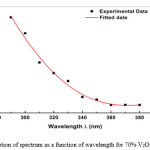 |
Figure 1: Absorption of spectrum as a function of wavelength for 70% V2O5_30%Bi2O3 film. Click here to View figure |
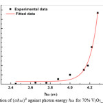 |
Figure 2: Variation of against photon energy for 70% V2O5_30%Bi2O3 film. Click here to View figure |
The result in Fig1 also follows the Urbach law [3]:
![]()
Where is the extent of band tailing due to presence of localized states, arising from of long- rang order.
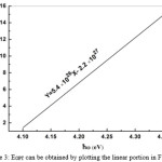 |
Figure 3: EOPT can be obtained by plotting the linear portion in Fig 2. |
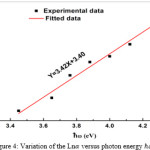 |
Figure 4: Variation of the Ln versus photon energy hω Click here to View figure |
As can be seen from Fig3 the EOPT is equal to about 4.07(ev) and the value of B in equation (1) is found to be about 5.4 ( ). Fig 4 shows that graph of Ln versus photon energy is linear at higher photon energies.
There have been a number of different interpretations of the origin of the exponential
dependence of on photon energy. On is based on the presence of strong internal electric fields due to structural disorder [4], while another says that it is due to electronic transitions between localized states in the band gap tails where the density of states falls of exponentially with energy. Mott and Davis [5] rejected the latter interpretation because the slopes of the exponential absorption edge are much the same in a variety of materials.
Conclusion
The energy band gaps of V2O5-Bi2O3 thin film chalcogenide glasses have been studied at room temperature and normal pressure. The reflections spectra of these glasses are recorded by Spectrophotometer in the wave length region from 200 to 800 nm. From the analysis of the reflection spectra the optical energy band gap is determined. It is also found that the optical energy gap EOPT is about 4.07 eV and the mechanism of transition is direct forbidden transition. It will be necessary to conduct thermo power and ESR experiments to verify this tentative conclusion.
References
- Davis E. A. and Mott N. F. Phill.Mag. 22, 903 (1970).
- Tauc J., Grigorivici R. and Vancu A., Phys.Status Solidi 15, 627 (1966).
- Urbach,F.,Phys.Rev.92(1953)1342.
- Dow J. D. and Redfild D., Phys.Rev.135, 594 (1972).
- Mott N. F. and Davis E. A., Electronic Processes in non-crystalline materials(Clarendon Press, Oxford, 1979).
- Singh K., Saxena N. S, Srivastava O. N., Patidar D., Sharma T. P., Chalcogenide Letters Vol. 3, No. 3, 33 – 36 (2006).
- Reyes-Coronado1 D., Rodr´ıguez-Gattorno1 G., Espinosa-Pesqueira M. E., Cab C., de Coss R. and Oskam G. , Nanotechnology 19, 145605 (2008).
- Nakayama N. and Hayashi T. , Colloids and Surfaces A: Physicochem. Eng. Aspects 317, 543–550 (2008).

This work is licensed under a Creative Commons Attribution 4.0 International License.
![]()
A New Edition of Web of Science
Journal Impact Factor
2022: 0.5
Five Year: 0.8
Journal is Indexed in

Cabells Whitelist
![]()


