Effect of Annealing on the Activation Energy of Thin Films of Manganese Sulphide, Copper Phthalocyanine and Multilayer Manganese Sulphide-Copper Phthalocyanine from their Electrical Studies
Shaji Varghese1 and Mercy Iype2
1Department of Physics, St.Thomas College,Kozhencherry, Kerala (India).
2Department of Chemistry, Marthoma College,Tiruvalla, Kerala (India).
Manganese Sulphide (MnS) thin films are prepared onto glass substrates by chemical bath deposition (CBD) technique. Thin films of Copper phthalocyanine (CuPc) are also sublimed onto glass substrates in high vacuum at room temperature. Multi layer MnS- CuPc thin films are obtained from MnS films grown on glass substrates by CBD technique and subsequently vacuum subliming CuPc onto them. These films are annealed in air at different temperatures. Electrical conductivity studies are made separately on MnS, CuPc and multi layer MnS-CuPc thin films. Thermal activation energy of the as deposited and annealed samples are determined from the Arrhenius plot. It is found that the activation energy decreases with annealing temperature. This may be due to the reduction in trap sites during annealing.
KEYWORDS:Annealing; Activation Energy; Thin Filsm; Electrical Studies
Download this article as:| Copy the following to cite this article: Varghese S, Iype M. Effect of Annealing on the Activation Energy of Thin Films of Manganese Sulphide, Copper Phthalocyanine and Multilayer Manganese Sulphide-Copper Phthalocyanine from their Electrical Studies. Orient J Chem 2011;27(1). |
| Copy the following to cite this URL: Varghese S, Iype M. Effect of Annealing on the Activation Energy of Thin Films of Manganese Sulphide, Copper Phthalocyanine and Multilayer Manganese Sulphide-Copper Phthalocyanine from their Electrical Studies. Orient J Chem 2011;27(1). Available from: http://www.orientjchem.org/?p=24843 |
Introduction
In the search for low-cost solar energy materials, organic – inorganic photovoltaic junctions in thin-film configuration deserves great attention. The first observations in this field have been made on inorganic semiconducting crystals by Horowitz and Garnier [1] who have investigated the GaAs-PT (PT=poly thiophene) n-p hetero junction, followed by Frank et al.[2] who studied the CdS- PMeT ( PMeT= poly(3-methylthiophene)) Schottky junction. In both the cases the polymer was electrochemically grown on single crystals of the inorganic semi conductors. Later, investigations were done on thin films CdS-PMeT solid state junctions [3-7]. P.Chartier et al studied the hybrid organic-inorganic photovoltaic junction of CdSe- poly(3-methylthiophene) thin films [8].
MnS has a direct band gap and can be used as window material in photovoltaic solar cells. Direct energy gap materials result in large optical absorption which in turn permits the use of thin layers of active material. The semiconducting nature of MnS films is found to be p-type.[9]
Phthalocyanines are one of the most widely investigated group of materials due to their potential applications as organic dyes, organic photoconductors, and gas sensors.[10-12]. These organic semiconductors exhibit high chemical and thermal stability. Semiconducting behaviour of all phthalocyanine films is found to be P-type at all temperatures[13].
Experimental Details
Preparation of MnS thin films
Chemical bath deposition (CBD) is a technique for controlling the homogeneous precipitation of water insoluble compounds and their solid solution [22,23]. One of the advantages of CBD is that high quality films can be prepared on large area substrates and this may be called a “ zero energy ” deposition process. Another advantage of this technique is the convenience of dopping. In this paper we describe the chemical deposition of MnS thin films on pyrex glass substrates by the decomposition of thioacetamide in an alkaline solution containing a Manganese salt [24,25]. The chemical process consists of the slow release of Mn2+ and S2- ions in solution which subsequently condenses on an ion-ion basis on to the glass substrate.[26]
Stock solutions of 1M Manganese sulfate and 1M thioacetamide are prepared in tridistilled water[27,28]. A 100 ml deposition bath is prepared by the sequential addition of the following. 15 ml of 1M Manganese sulfate, 4.4 ml of NH3 / NH4Cl (PH 10), 5.4 ml of 50% triethanolamine, 15 ml of 1 M thioacetamide, and the rest deionized water to make upto 100 ml by volume. The glass slides are washed with detergent solution, then with chromic acid and finally rinsed with de ionised water prior to the deposition of the films. Cleaned glass slides are kept vertically on the walls of the container with the deposition mixture. Depositions are done at room temperature for 24 hours. The films are dried in air.
Preparation of CuPc and multi layer MnS-CuPc thin films
The copper phthalocyanine (CuPc) powder used in this study is obtained from Aldrich chemical company Inc: USA( 97.99% pure) . Thin films of CuPc are deposited at room temperature on to glass substrates and MnS coated glass substrates at a base pressure of 10-5 Torr using a Hind Hivac Vacuum coating unit. The evaporation is carried out by resistive heating of the CuPc powder from a molybdenum boat and the rate of sublimation is kept constant. [29].
Thickness of the films are accurately determined by Tolanskys multiple beam interference technique [30]. Electrical conductivity is measured using the standard two probe method with a programmable Keithley electrometer (Model No. 617) and a constant current source. Ohmic contacts are made by thin copper strands which are fixed by Silver paste. The film is loaded on the hollow copper block of the conductivity cell. Conductivity measurements are performed in the temperature range 320-505K under a vacuum of 10-3 Torr to avoid any type of contamination. Temperature is monitored using a Chromel-Alumel thermocouple attached to the substrate.
Results and discussions
Electrical studies are done to determine the thermal activation energy and the effect of annealing on activation energy. The studies are carried out in the temperature range 320-505 K in a vacuum of 10-3 Torr to avoid contamination of the film. The resistance R is noted at regular intervals of 5K.
The temperature dependance on resistance is expressed as,R = Ro exp (-Ea/ KT)
where Ea is the thermal activation energy and K is the Boltzmann constant.
The activation energy is obtained using the relation,s δ = δ o exp ( – DEa/ KT )
where s is the carrier conductivity, DEais the activation energy, K is the Boltzmann constant and T is the temperature in absolute scale. The electrical conductivity as a function of inverse of temperature of as deposited and annealed MnS films are given in Fig.1. Fig.2 represents similar plots of as deposited and annealed samples of CuPc films. Fig.3 gives plots of as deposited and annealed samples of multi layer MnS-CuPc. From the slopes of these graphs, activation energies are determined. The activation energy of the samples varies with annealing temperature. Each graph has three linear regions which give E1 ,E2 ,and E3 . The activation energies in the intrinsic region (E1 ) and impurity scattering regions ( E2 and E3 ) are calculated. Tables I, II & III represents variation of activation energies with annealing temperatures for MnS, CuPc and multi layer MnS-CuPc films respectively. The change in carrier activation energy is indicated by the change in the slope of the plot. Multiple donor and acceptor levels exist within the forbidden energy gap and as temperature is lowered the deeper levels become progressively frozen out. The activation energy measurements provide a measure of the trapping levels. It has been reported that the removal of oxygen causes a redistribution of traps and hence a drop in thermal activation energy [31]. Sussman has reported that the distribution of trapping sites is altered by annealing [32].
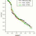 |
Figure 1: Graph of Electrical conductivity Vs inverse of temperature of as deposited and annealed MnS thin films |
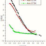 |
Figure 2: Graph of Electrical conductivity Vs inverse of temperature of as deposited and annealed CuPc thin films. |
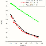 |
Figure 3: Graph of Electrical conductivity Vs inverse of temperature of as deposited and annealed multi layer MnS- CuPc thin films. |
Table 1:Variation of Activation Energy with annealing temperature for MnS films of thickness 3515 A.
| Samples | Activation energy ( ev )
E1 E2 E3 |
| 1. As deposited
2. Annealed 523 K
3. Annealed 573 K
|
0..3323 0.2415 0.1974
0.3181 0.2070 0.1391
0.2940 0.1961 0.1378 |
Table 2: Variation of Activation Energy with annealing temperature for CuPc films of Thickness 2180 A.
| Samples | Activation energy ( ev )
E1 E2 E3 |
2. Annealed 523 K
3. Annealed 573 K
|
0.7065 0.6091 0.1851
0.5859 0.5803 0.1725
0.5003 0.2710 0. 0551 |
Table 3: Variation of Activation Energy with annealing temperature for Multi layer MnS-CuPc films of thickness 6630 A.
| Samples | Activation energy ( ev )
E1 E2 E3 |
2. Annealed 523 K
3. Annealed 573 K
|
0.7991 0.5476 0.1949
0.6086 0.5403 0.1894
0.3525 0.3269 0.1860 |
Conclusion
Manganese Sulphide thin films are prepared on glass substrates by chemical bath deposition method. Thin films of Copper Phthalocyanine are sublimed onto glass substrates in high vacuum at room temperature. Multi layer MnS-CuPc thin films are obtained from MnS films grown on glass substrates by CBD technique and subsequently vacuum subliming CuPc onto them. Electrical conductivity and thermal activation energy of the as deposited and annealed MnS, CuPc and multi layer MnS-CuPc thin films have been studied. Electrical conductivity by thermal activation process is found to involve different conduction mechanisms. For CuPc in the high temperature range, intrinsic conductivity by holes are found to contribute to the conduction process whereas in the low temperature range impurities are found to play an active role. Annealing causes the reduction in activation energy for all the films. This may be due to the reduction in trap sites because of annealing.
References
- G. Horowitz, F.Garnier, Solar Energy Materials. 1986,13 , 47.
- A.J. Frank, S. Glenis, A.J. Nelson, J.Phys. Chem. 1989, 93, 3818
- P. Chartier,B. Ba, J. Ebothe,N. Alonso Vante, H. Nguyen Cong, J.Electroanal.Chem., 1982,138, 381.
- C. Bouchenaki, B. Ullrich, J.P. Zielinger, H. Nguyen Cong, P. Chartier, J. Crystal Growth, 1990, 101, 797.
- C.Sene, H. guyen Cong, P. Chartier, J. Mater. Sci: Mater. In Electronics,1997,8, 85.
- H. Nguyen Cong, C. Sene, P.Chartier, Sol. Energy Mater. Sol. Cells,1996,40, 261.
- H. Nguyen Cong, C. Sene, P.Chartier, Sol. Energy Mater. Sol. Cells,1993,30, 209.
- P.Chartier, H. Nguyen Cong, C.Sene, Sol. Energy Mater. Sol. Cells,1998,52, 413.
- K.Okamoto, S.Kawai, Jpn. J.Appl.phys., 1973,12 ,1130; P.K.Nair,M.T.S.Nair et al./ Sol. Energy Mater. Sol. Cells, 1998, 52, 313-344.
- K. Nebesny, G.E.Collins, P.A.Lee, Chem.Mater,1991,3, 829.
- M.Pope, C.E.Swenberg, ElectronicProcessing anic Crystals,Clarendoness,Oxford, 1992.
- C.W.Tong, Appl. Phys. Lett.,1986,48,183.
- Y. Sadaoka, T.A. Jones, W. Gopel, J. Mater. Sci. Lett.,1989,8, 1095.
- H.Cachet, h. Essaaidi, M.Froment, G.Maurin, J.Electroanal. Chem., 1995,396,175.
- S. Gorer, G. Hodes, J.Phys. Chem., 1994,98,5338.
- M.T.S.Nair, P.K.Nair, H.M.K.K.Pathiarana, R.A.Zingaro,E.A.Meyers, J.Electrochem.Soc.,1993,140, 2987.
- J.M.Gracia-Jimenez,G.Martinez- Montes,R.SilvaGonzales,J.Electrochem.Soc.,1992,139, 2048.
- K.C. Mandal, O.Savadogo, J. Mater.Sci. Lett.,1991,10, 1446.
- Y.Ueno, H.Kaigawa, T.Ohashi, T.Sugiura, H.Minoura,Sol.Energy Mater.,1987,15,421.
- R.A.Boudreau, R.D.Rauh,J.Electrochem. Soc., 1983,130, 513.
- D.R.Pratt ,M.E.Langmuir, R.A.Boudreau, R.D.Rauh, J.Electrochem. Soc,1981,128, 1627
- K.L.Chopra,R.C.Kainthla,D.K.Pandya,A.P.Thakoor,in:G.,Hass,M.H.Francombe, J.L.Vossen(Eds.),Physics of Thin Films, vol.12,Academic Press, New York, 1982,p.201.
- Polyvyannyi . J. Russ, In org. Chem: , 1981,26, 561
- P.K. Nair, M.T.S. Nair, Solar cells, 1987,22, 103
- O.Savadogo, K.C.Mandal, J. Electro chem. Soc.,1994,14,32pp
- O.Savadogo,Solar energy materials and solar cells, 1998,52, 361-388.
- O.Savadogo, K.C.Mandal, Apply.Phys.Lett.,1993,63, 12.
- O.Savadogo, K.C.Mandal, J. Electro chem. Soc.,1994,141,2871.
- S.Ambily, C.S.Menon, Sol. Stat. Commun., 1995,94, 485.
- L.I.Maissel, R.Glang,Handbook of Thin Film Technology, McGraw-Hill,1983,p.11-18.
- A.Epstein, B.S.Wildi, J.Chem.Phys., 1960,32, 324
- A.Sussman, J. Appl.Phys.,1967,38, 2748.
- F. Garnier, La Recherche,Paris, 1996,184, 20.

This work is licensed under a Creative Commons Attribution 4.0 International License.
![]()
A New Edition of Web of Science
Journal Impact Factor
2022: 0.5
Five Year: 0.8
Journal is Indexed in

Cabells Whitelist
![]()


