Raman Investigations of Metal Chalcogenide Thin Films (A Short Review)
Ho Soonmin*
Centre for Green Chemistry and Applied Chemistry, INTI International University, Putra Nilai, 71800, Negeri Sembilan, Malaysia.
Corresponding Author E-mail: soonmin.ho@newinti.edu.my
DOI : http://dx.doi.org/10.13005/ojc/35Specialissue101
Article Received on : 26-12-2018
Article Accepted on : 01-02-2019
Article Published : 20 Mar 2019
Preparation and characterization of thin films have been reported by many researchers. Research of nanostructured thin films has recently received great attention due to their specific properties. The films obtained can be used for the development of optoelectronic, solar cells, laser devices and gas sensor. Several methods (X-ray diffraction, scanning electron microscopy, x-ray photoelectron spectroscopy, UV-Visible spectrophotometer, transmission microscopy and Fourier Transform Infrared spectroscopy) have been employed to study the materials in terms of structural, morphological, compositional, optical and electrical properties. In this short paper, Raman spectroscopy was used to characterize the properties of thin films. There are very clear advantages and disadvantages of this tool that need to be considered when using it. The obtained results highlight Raman spectra were used to confirm the purity of sample and the phase identification.
KEYWORDS:Band Gap; Raman Spectroscopy; Semiconductor; Solar Cells; Thin Films
Download this article as:| Copy the following to cite this article: Soonmin H. Raman Investigations of Metal Chalcogenide Thin Films (A Short Review). Orient J Chem 2019;35(Special Issue 1 Spectroscopy March 2019). |
| Copy the following to cite this URL: Soonmin H. Raman Investigations of Metal Chalcogenide Thin Films (A Short Review). Orient J Chem 2019;35(Special Issue 1 Spectroscopy March 2019). Available from: https://bit.ly/2HunBqN |
Introduction
The binary,1-8 ternary,9-15 quaternary16-18 and penternary compounds19-22 have received great attention owning to their unique properties. These films are used in a wide variety of applications such as solar cell,23-25 sensors,26 photodiode arrays,27 photoconductors28 and optoelectronic devices.29 The chalcogen is the elements (oxygen, sulfur, selenium and tellurium) in Group 16 of the periodic table. The band gap energy was estimated to be in the range of 1-3 eV.30,31 Currently, the solar cell market is dominated by silicon solar cell32 due to abundant, non-toxic33 and shown remarkably higher power conversion efficiency. However, these solar cells are more expensive that other types of cells.34 Thin film solar cell has always been cheaper but less efficient. This solar cell is favorable due to its minimum material usage. The two major thin film technologies such as cadmium telluride and copper indium gallium diselenide successfully contributed about 10 % of the global production market share. The major drawback is high toxic material such as tellurium, cadmium,35 and selenium.
In this work, thin films were investigated using Raman spectroscopy. The purity of sample and the phase identification were also examined.
Literature Survey
Raman spectroscopy provides useful information on molecular interactions,36 crystallinity, crystal phase37 and chemical structure.38 Raman is based upon the interaction of light with the chemical bonds within a material. Raman spectra exhibit the intensity of the scattered photons versus the frequency difference to the incident photons. Typically, the peaks fall within a range of 500 to 2000 cm-1 and only appear if vibrational modes are sensitive to the laser wavelength used.39
Raman spectroscopy is chemical analysis technique40 and is employed to measure the scattering radiation41 of a matter (Figure 1). Generally, when light is scattered by matter, almost all of the scattering is an elastic process42 and does not give useful information (commonly known as Rayleigh Scatter). However, a very small percentage of scattering43 is an inelastic process (known as Raman effect). Raman spectroscopy is both qualitative (measuring the frequency44 of the scattered radiations) and quantitative (measurement of the analyte concentration in the sample by quantifying the intensity of the scattered radiations). The obtained Raman spectra give a unique data45,46 to identify a material and distinguish it from others. Table 1 shows the advantages and limitations of Raman spectroscopy technique.
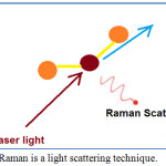 |
Figure 1: Raman is a light scattering technique. |
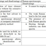 |
Table 1: Advantage and disadvantage of Raman spectroscopic.
|
Several efforts have been made by researchers to synthesize semiconductor thin films such as sulfur, selenium and tellurium-based nanostructured films. Typical deposition technique is shown in Table 2. In this study, the utilization of Raman spectroscopy for the characterization of thin films was discussed.
Table 2: Raman spectroscopic investigation of thin films prepared under various deposition conditions.
| Thin films | Raman spectroscopy explained | Deposition method | Reference |
| Binary thin films | |||
| Thalium selenide | TlSe2 bending mode at 92 cm-1Tl-Se symmetric stretching modes at 158 and 140 cm-1Tl-Se asymmetric stretching modes at 208 and 185 cm-1Se-Se stretching modes at 255 and 240 cm-1
In terms of crystal structure, Tl-Se bond was observed in 2.66-2.73 Å |
Thermal evaporation method | 51 |
| Arsenic triselenide (As2Se3) | The peak at 224 cm-1 corresponded to asymmetric (for amorphous phase)Weak peak at 480 cm-1 represented Se-Se vibrationThe peak at 221 cm-1 could be seen in In-doped As2Se3 filmsThere are two peaks at 216-219 cm-1 and 240-242 cm-1 for the films prepared with indium content of 2 %. | Thermal evaporation | 52 |
| Antimony triselenide (Sb2Se3) | Peak at 188 cm-1: Sb-Se stretching modePeak at 150 cm-1: Sb-Sb bondPeak at 120 and 210 cm-1: vibration mode Se-Se bondRaman spectra reflected selenium rich in sample (peaks at 70, 102, 129, 252 cm-1). | RF magnetron sputtering | 53 |
| Tungsten disulfide (WS2) | Peak at 175 cm-1 represented vibration modePeak at 419 cm-1 attributed to WS2 phase | Pulsed laser deposition | 54 |
| SnS2 films | Citric acid was used as complexing agent during the deposition process.The films prepared using 0.375, 0.5 and 0.625 ml/L citric acid indicated the peak at 315 cm-1 (mode of hexagonal SnS2 phase).Researchers confirm the phase purity of sample. | Chemical bath deposition | 55 |
| SnS | The peak was observed at 307 cm-1 for the films prepared using 40 and 50 mTorr, indicating that the formation of Sn2S3.There are two peaks (93 and 224 cm-1) could be seen for the films prepared using 6 and 10 mTorr, respectively.An additional small peak in the spectra (135 cm-1) was detected for the films synthesized under 40, and 50 mTorr. | RF sputtering | 56 |
| FeS2 | There are two main phases (pyrite [343, 379 & 430 cm-1] and marcasite [323 & 386 cm-1]) of development for the synthesis of iron sulphide.Pyrite was preferentially produced (pyrite:marcasite about 99:1) at high temperature (420 °C).At low deposition temperature (250 °C), marcasite was grown preferentially. | Evaporation method | 57 |
| InS | There are very broad peaks at 200-500 cm-1 may indicate the presence of amorphous or nano crystalline materials.Researchers were able to identify some peaks at 200-400 cm-1 contributed to the In2S3 Peak at 460 cm-1 attributed to the S-S mode of sulphur | Chemical bath deposition | 58 |
| In2S3 | There are 3 peaks (115, 135 and 180 cm-1) could be observed for the films prepared at 60, 70 and 80°C.The presence of In2O3 could be detected for the films deposited at 60°CThe intensity of peak is improved in annealed films. | Chemical bath deposition | 59 |
| As2S3 | There are 3 peaks (336, 230, 485 cm-1) could be seen for the films prepared using laser lightPeaks at 335-340 cm-1 associated with As-S bond stretching vibration (pyramidal phase).Peaks at 180 and 230 cm-1 attributed to As-As homopolar bond vibrationPeak at 485 cm-1 corresponded to S-S vibration of AsS4 | Thermal evaporation | 60 |
| CdTe | Both the transverse (142 cm-1) and longitudinal (170.5 cm-1) mode could be found.Peak at 120 cm-1 attributed to phonon of tellurium | Thermal evaporation | 61 |
| ZnS films | Two peaks at 773 and 1078 cm-1 were detected in annealed and as-deposited films.The lattice constant value for both as-deposited (5.3 Å) and annealed films (5.66 Å) was determined. | Physical vapor deposition | 62 |
| Bi2Te3 | Peak at 77 cm-1 attributed to vibration mode of BiTePeaks at 65 and 131 cm-1 due to vibration mode of trigonal directionPeak at 102 cm-1 corresponded to vibration mode in the basal plane | Electro deposition | 63 |
| CdS | Three peaks (299, 600 and 900 cm-1) were found and could be observed as longitudinal optical phonons. | Chemical bath deposition | 64 |
| CdS | There are 2 peaks could be identified (296 and 593 cm-1), for the films prepared under various pH values.The intensity of the Raman peak decreases with increasing the pH value from pH 9 to 11. | Chemical bath deposition | 65 |
| Ternary thin films | |||
| Ag-Ge-Se | The films showed GeSe4/2 corner sharing tetrahedral at 192-201 cm-1, vibration of Se atom at 210-218 cm-1, Se-Se bond at 255-270 cm-1 and Ge-Ge mode at 178 cm-1 | Pulsed laser deposition | 66 |
| Ge-Sb-Se | Four main modes such as symmetric stretching mode of GeSe4/2 tetrahedral (200, 215 cm-1), stretching mode of Ge-Ge bond (170 cm-1), Se-Se stretching mode (235-245 cm-1) and Se-Se bond vibration (265 cm-1) are observed in these films | RF magnetron sputtering | 67 |
| Ge2Sb2Te5 | They observe some peaks such as 80 (GeTe4 tetrahedral), 125 (GeTe4-nGen(n=1,2)), 153 (presence of Sb2Te3) and 300 cm-1 (presence of Ge-Ge) in spectra | Thermal evaporation | 68 |
| GexAs35-xSe65 | The films exhibited symmetric vibrational stretching GeSe4/2 at 198 cm-1, vibration mode of AsSe3/2 at 230 cm-1, vibration mode of selenium at 260 cm-1 and vibration mode of GeSe4/2 tetrahedral at 215 cm-1 | Thermal evaporation | 69 |
| As50Se40Te10 | Three major modes such as asymmetric stretching As-Te-Se mode (127 cm-1), As-Se vibration mode (228 cm-1) and Te-Te vibrational mode (472 cm-1) are observed in these films | Thermal evaporation | [70] |
| Cu2SnS3 | The Raman peaks exhibit strong (vibration mode in monoclinic) and weak peak (Cu2SnS3 phase). | Evaporation method | 71 |
| CuSbSe2 | They observe several peaks such as 188, 250, 372, 450 cm-1 (Sb2Se3), 185 cm-1 (Cu3SbSe3), and 82, 117, 144 cm-1 (presence of CuSbSe2) in spectra | E-beam evaporation deposition | 72 |
| Cu12Sb4S13 | There are many peaks such as 351 cm-1 (Cu12Sb4S13),354 cm-1 (Sb-S bond stretching), 315 cm-1 (Sb-S bond bending mode), 330 cm-1 (Cu3SbS4), 468 cm-1 (CuS) could be confirmed. | e-beam evaporation | 73 |
| Cu2SnS3 | There are several peaks could be identified such as 290 and 350 cm-1 (monoclinic), 325 cm-1 (tetragonal phase), 223 and 371 cm-1 (Cu2Sn3S7) | Radio frequency magnetron sputtering | 74 |
| Cu2SnS3 | The films indicated orthorhombic Cu3SnS4 phase at 295 cm-1, monoclinic Cu2SnS3 at 289 cm-1 and vibration mode of tetragonal Cu2SnS3 in anneal films at 326 cm-1 | Spray pyrolysis | 75 |
| Cu2SnSe3 | Peak at 2926 cm-1 was observed (attributed to C-H stretching vibration of CH2) for the films prepared using 0.5 M of sodium citrate.However, this peak could not be detected when using higher concentration (0.1 M). | Electro deposition | 76 |
| Quaternary thin films | |||
| Cu2ZnSnS4 | The films showed a prominent kesterite phase (331-336 cm-1), indicating microwave treatment enhanced nucleation and grow process. | Sol gel method | 77 |
| Cu2ZnSnS4 | There is no Raman peak could be detected for the films prepared at room temperature and within the first 15 minutes.The films prepared under 30 minutes of sulfurization show peak at 330 cm-1The films synthesized under 60 and 180 minutes of sulfurization show higher intensities if compared to other conditions.There are no other impurities (ZnS, SnS2 and CuS) indicating high purity of sample. | Sol gel technique | 78 |
| Cu2FeSnS4 | Two main modes such as sulfur pure anion around the copper metal (285 cm-1) and asymmetry vibration mode of sulphur around the tin metal (319 cm-1) are observed in these films. | Spray pyrolysis | 79 |
| CuGaxIn1-xSe2 | The presence of Cu2Se (290 cm-1) and Cu(In,Ga)Se2 phase (175 cm-1) could be detected when x=1, and x=0, 0.3, respectively. | Close spaced vapor transport technique | 80 |
| Cu2ZnSnS4 | Kesterite phase (332, 285, 356 and 368 cm-1), copper tin sulphide (303 cm-1) and copper sulphide (468 cm-1) were observed in Raman spectra. | Spray pyrolysis | 81 |
| CuIn(S,Se)2 | There are many peaks at 473 cm-1 (Cu2-xS), 390-475 cm-1 (sulfur rich Cu2-x(S,Se)), 228 cm-1 (CuIn3Se5) and 150-400 cm-1 (amorphous In2S3)could be confirmed. | Chemical bath deposition | 82 |
| Penternary thin films | |||
| Cu2ZnSn(S,Se)4 | Raman study confirmed existence of the Cu2ZnSnSe4 (196 cm-1), Cu2ZnSnS4 (338 cm-1) and CZTSSe films (202 and 329 cm-1). | Spin coating technique | 83 |
| Cu2ZnSn(S,Se)4 | Raman investigation showed existence of the polycrystalline filmsStrong peaks could be seen at 196 (vibration with asymmetry of CZTSe) and 338 cm-1 (vibration with asymmetry of CZTS).Cu2ZnSnS4 (CZTS) shows narrow peak, however Cu2ZnSnSe4 (CZTSe) exhibits broad peak as the concentration of H2S was increased from 1 to 5 %. | Co-evaporation technique | 84 |
| Cu2ZnSn(S,Se)4 | CZTS has three peaks (288, 337 and 367 cm-1), while CZTSSe has two peaks (208 and 329 cm-1).Pure CZTSSe phase was confirmed. | Successive ionic layer adsorption and reaction | 85 |
| Cu2ZnSn(SxSe1-x)4 | Two strong peaks at 336 cm-1 (CZTS) and 195 cm-1 (CZTSe) could be identified.They report that most of the peaks shift to lower frequency due to selenium replaced sulfur in samples. | Solvothermal method | 86 |
Conclusion
Raman spectroscopy is a powerful technique for characterization of thin films. Here, author reviews the Raman spectra of nanostructured films. Also, author indicates how to use it to determine structure and composition of samples. The purity of the compound and phase formation can be verified by this technique.
Acknowledgements
INTI International University is gratefully acknowledged for the financial support of this work.
Conflict of Interest
There is no conflict of interest.
References
- Khadher, A.; Mazahar, F.; Gulam, R. Oriental J. Chem., 2018, 34, 2203-2207.
- Mohd, J.H.; Mohd, Y.R.; Ho, S.M.; Anuar, K.; Abdul, H.A.; Saravanan, N. Kuwait J. Sci. Eng., 2010, 37, 63-73.
- Gao, C.; Xu, M.; Ng, B.K.; Kang, L.; Jiang, L.; Lai, Y.; Liu, F. Mater. Lett., 2017, 195, 186-189.
- Tan, W.T.; Ho, S.M.; Anuar, K., Saravanan, N. Eur. J. Appl. Sci., 2011, 3, 75-80.
- Shanmugasundaram, K.; Thirunavukkarasu, P.; Ramamurthy, M.; Balaji, M.; Chandrasekaran, J. Oriental J. Chem., 2017, 33, 2484-2491.
- Victor, R.; Juan, F.T.; Cecilia, G.; Jose, H. Thin Solid Films, 2015, 582, 249-252.
- Kassim, A.; Ho, S.M.; Tan, W.T.; Shanthi, M.; Saravanan, N. Kathmandu Univ. J. Sci. Eng. Technol., 2010, 6, 126-132.
- Sakthivel, R.; Ganesh, A.S.; Geetha, A.; Anandh, B.; Kannusamy, R.; Tamilselvan, K. Oriental J. Chem., 2017, 33, 355-362.
- Meena, S.P.; Ashokkumar, R. Oriental J. Chem., 2018, 34, 1884-1889.
- Sarwan, B.; Aman, D.A. Oriental J. Chem., 2018, 34, 2667-2670.
- Soepardjo, A.H. Makara Sains, 2009, 13, 200-204.
- Kanakaraj, M.; Ramalingam, H.B. Oriental J. Chem., 2017, 33, 2899-2904.
- Anuar, K.; Saravanan, N.; Ho, S.M.; Tan, W.T.; Atan, S.; Zulkefly, K. Chiang Mai Univ. J. Nat. Sci., 2008, 7, 317-326.
- Chalapathi, U.; Poornaprakash, B.; Park, S. Ceram. Int., 2017, 43, 5229-5235.
- Ho, S.M. Oriental J. Chem., 2014, 30, 1009-1012.
- Li, X.; Cao, H.; Dong, Y.; Yue, F.; Chen, Y.; Xiang, P.; Sun, L.; Yang, P.; Chu, J. J. Alloys Compd., 2017, 694, 833-840.
- Soumyo, C.; Amlan, J.P. Sol. Energy Mater. Sol. Cells, 2017, 160, 233-240.
- Dong, L.; Cheng, S.; Lai, Y.; Zhang, H.; Jia, H. Thin Solid Films, 2017, 626, 168-172.
- Jakapan, C.; Takuya, K.; Hiroki, S.; Takashi, M. Curr. Appl. Phys., 2017, 17, 461-466.
- Gang, M.G.; Shin, S.W.; Hong, C.W.; Gurav, K.V.; Gwak, J.; Yun, J.H.; Lee, J.Y.; Kim, J.H. Green Chem., 2016, 18, 700-711.
- Yang, K.; Sim, J.; Son, D.; Kim, Y.; Kim, D.; Nam, D.; Cheong, H.; Kim, S.; Kim, J.; Kang, J. Nano Energy, 2017, 35, 52-61.
- Lv, X.; Wang, J.; Zhu, C.; Wang, Z. Rare Metals, 2016, 35, 718-722.
- Wie, W.; Mark, T.W.; Oki, G.; Tayfun, G.; Teodor, K.T.; Yu, Z.; David, B.M. Adv. Energy Mater., 2014, https://doi.org/10.1002/aenm.201301465.
- Kassim, A.; Ho, S.M.; Saravanan, N.; Noraini, K. Arabian J. Chem., 2010, 3, 243-249.
- Ngai, C.F.; Anuar, K.; Ho, S.M.; Tan, W.T. Am. J. Appl. Sci., 2011, 8, 359-361.
- Ogita, M.; Higo, K.; Nakanishi, Y.; Hatanaka, Y. Appl. Surf. Sci., 2001, 175-176, 721-725.
- Saxena, R.S.; Aparna, S. Infrared Phys. Technol., 2014, 65, 51-53.
- Ren, Y.X.; Dai, T.J.; Luo, W.B.; Liu, X.Z. Vacuum, 2018, 149, 190-194.
- Hosein, K. Ceram. Int., 2019, 45, 334-345.
- Ashwini, B.R.; Priyanka, U.L.; Jeong, I.H.; Nandu, B. C. Appl. Surf. Sci., 2019, 466, 358-366.
- Seyed, M.M.; Hosein, K. Superlattices Microstruct., 2019, 126, 139-149.
- Green, M.A.; Basore, P.A.; Chang, N.; Clugston, D.; Egan, R.; Hogg, D.; Jarnason, S. Sol. Energy, 2004, 77, 857-863.
- Gavin, C.; Green, M.; Corkish, R.; Cho, Y.; Cho, E.; Jiang, C.; Thipwan, F. Thin Solid Films, 2006, 511-512, 654-662.
- Saga, T. NPG Asia Mater., 2010, 2, 96-102.
- Fahhad, A.; John, D.B.; Salhi, A.; Ahmed, A.; Kim, H.; Miller, R.D. Renew. Energy, 2011, 36, 2753-2758.
- Amer, M.S. Raman spectroscopy for soft matter applications. John Wiley & Sons Inc: New Jersey, 2009.
- Challa, S. Raman spectroscopy for nanomaterials characterization. Springer Science & Business Media: Berlin, 2012.
- Mantz, R.A. Molten salts XIV: Proceedings of the International Symposium, The Electrochemical Society: New Jersey, 2006.
- Zhang, S. Raman spectroscopy and its application in nanostructures. John Wiley & Sons, Inc: New Jersey, 2012.
- Ewen, S.; Dent, G. Modern Raman spectroscopy: A practical approach. John Wiley & Sons, Inc: New Jersey, 2005.
- Peter, L. Infrared and Raman spectroscopy: Principles and spectral interpretation. 2nd edition, Elsevier: Amsterdam, 2018.
- John, C.L. Rayleigh scattering and Raman spectroscopy, theory. Encyclopedia of Spectroscopy and Spectrometry, Elsevier: London, 2000.
- Shadi, A.D.; Anna, F.; Chennupati, J. Semiconductor nanowires II: properties and applications. Elsevier: London, 2016.
- John, R.F.; Kazuo, N. Introductory Raman spectroscopy. Academic Press Inc, New York, 1994.
- Fasolato, C. Surface enhanced Raman spectroscopy for biophysical applications: using plasmonic nanoparticle assemblies. Springer: Berlin, 2018.
- Alan, C. Biophysical chemistry, Royal Society of Chemistry: London, 2004.
- Weber, W.H.; Merlin, R. Raman scattering in materials science, Springer-Verlag: Berlin, 2000.
- High Pressure studies of crystalline materials. MDPI: Basel, 2018.
- Ian, R.L.; Howell, E. Handbook of Raman spectroscopy: from the research laboratory to the process line. Marcel Dekker Inc: New York, 2001.
- Sasic, S. Pharmaceutical applications of Raman spectroscopy. A John Wiley & Sons, Inc: New Jersey, 2008.
- Ozel, A.E.; Deniz, D.; Sefa, C.; Sahin, Y.; Binnur, K.; Sevim, A.; Kemal, U. Physica B: Condens Matter, 2017, 527, 72-77.
- Yuriy, A.; Volodymyr, D.; Dmytro, S.; Vasyl, L.; Laroslav, G.; Vasyl, L.; Alexander, G.; Dietrich, R.T. Appl. Surf. Sci., 2019, 471, 943-949.
- Shongalova, A.; Correia, M.R.; Teixeira, J.P.; Leitao, J.P.; Gonzalez, J.C.; Ranjbar, S.; Garud, S.; Vermang, B.; Cunha, J.; Salome, P.; Fernandes, P. Sol. Energy Mater. Sol. Cells, 2018, 187, 219-226.
- Kun, T.; Tiwari, A.; Baskaran, K. Thin Solid Films, 2018, 668, 69-73.
- Jing, L.; Yong, C.; Zhang, M. Mater. Sci. Forum, 2010, 663-665, 104-107.
- Vinaya, K.A.; Shin, Y.; Kim, J. Superlattices Microstruct., 2018, 122, 253-261.
- Walimbe, A.; Wertheim, A.; Ravi, A.; Kopas, C.; Saxena, A.; Singh, R.K.; Lehner, S.W.; John, D.; Makar, J.; Carpenter, R.W.; Buseck, P.R.; Newman, N. Thin Solid Films, 2019, 669, 49-55.
- Asenjo, B.; Guillen, C.; Chaparro, A.M.; Saucedo, E.; Bermudez, V.; Lincot, D.; Herrero, J.; Gutierrez, M.T. J. Phys. Chem. Solids, 2010, DOI: doi:10.1016/j.jpcs.2010.09.011.
- Rodriguez, P.E.; Flores, F.D.; Cervantes, A.; Campos, E.; Cruz, J.; Mayen, S. Chalcogenide Lett., 2016, 13, 389-396.
- Azhniuk, Y.; Dmytro, S.; Loya, V.; Iaroslav, G.; Vasyl, L.; Gomonnai, A.V.; Zahn, D. Appl. Surf. Sci., 2019, 467-468, 119-123.
- Mitric, J.; Paunovic, N.; Mitric, M.; Vasic, B.; Ralevic, U.; Trajic, J.; Romcevic, M.; Dobrowolski, W.D.; Yahia, I.S.; Romcevic, N. Physica E Low Dimens Syst Nanostruct., 2018, 104, 64-70.
- Keshav, R.; Mahesha, M.G. Mater. Res. Bull., 2018, 105, 360-367.
- Thorat, J.B.; Mohite, S.V.; Bagade, A.A.; Shinde, T.J.; Fulari, V.J.; Rajpure, K.Y.; Shinde, N.S. Mater. Sci. Semicond. Process., 2018, 79, 119-126.
- Oladeji, I.O.; Chow, L.; Liu, J.R.; Chu, W.K.; Bustamante, A.; Fredricksen, C.; Schulte, A.F. Thin Solid Films, 2000, 359, 154-159.
- Kariper, A.; Guneri, E.; Gode, F.; Gumus, C. Chalcogenide Lett., 2012, 9, 27-40.
- Erazu, M.; Rocca, J.; Fontana, M.; Urena, A.; Arcondo, B.; Pradel, A. J. Alloys Compd, 2010, 495, 642-645.
- Baudet, E.; Cardinaud, C.; Girard, A.; Rinnert, E.; Michel, K.; Bureau, B.; Nazabal, V. J. Non Cryst. Solids, 2016, 444, 64-72.
- Veres, M.; Kozyukhin, S.; Ingram, A.; Nguyen, H.P.; Kudoyarova, V. Phys. Proc., 2013, 44, 82-90.
- Khan, P.; Arinjoy, B.; Abin, J.; Vasant, S.; Uday, D.; Adarsh, K.V. Thin Solid Films, 2017, 621, 76-83.
- Mukta, B.; Naik, P.; Panda, R.; Naik, R. Opt. Mater., 2017, 66, 616-622.
- Kim, Y.; Choi, I. Thin Solid Films, 2019, 669, 351-354.
- Knal, J.T.; Vinod, V.; Subrahmanyam, A.; Malar, P. Appl. Surf. Sci., 2017, 418, 216-224.
- Kumar, D.S.; Ren, M.; Thomas, O.; Mallik, R.C.; Malar, P. Sol. Energy, 2018, 174, 422-430.
- Dong, Y.; Lu, X.; Shen, P.; Chen, Y.; Yue, F.; Xiang, P.; Sun, L.; Yang, P.; Chu, J. Mater. Sci. Semicond. Process, 2018, 84, 124-130.
- Biren, P.; Ranjan, K.P.; Indrajit, M.; Ray, A. Vacuum, 2018, 158, 263-270.
- Juskenas, R.; Zenius, M.; Raimondas, G.; Algirdas, S.; Giedrius, S.; Stase, K.; Audrius, D. J. Alloys Compd., 2018, 767, 345-352.
- Lei, Q.; Xu, J.; Cai, W.; Xie, Z.; Yang, Y. Superlattices Microstruct., 2019, 126, 83-88.
- Osama, A.; Zhe, C. Sol. Energy Mater. Sol. Cells, 2018, 176, 222-229.
- Chayma, N.; Mehdi, S.; Yvan, C.; Najoua, K. Superlattices Microstruct., 2018, 124, 17-29.
- Houda, T.; Bouloufa, A.; Marek, P.; Igalson, M. Mater. Sci. Semicond. Process, 2018, 88, 167-172.
- Sampath, M.; Sankarasubramanian, K.; Archana, J.; Hayakawa, Y.; Ramamurthi, K.; Sethuraman, K. Mater. Sci. Semicond. Process, 2018, 87, 54-64.
- Lugo, S.; Sanchez, Y.; Neuschitzer, M.; Xie, H.; Insignares, C.; Roca, V.; Pena, Y.; Saucedo, E. Thin Solid Films, 2015, 582, 74-78.
- Liu, Y.; Zhang, X.; Li, Q.; Long, M.; Hou, J.; Na, Z.; Zhao, G.; Fang, Y. J. Alloys Compd., 2017, 695, 3146-3151.
- Kim, Y., Choi, I. J. Korean Phys. Soc., 2017, 70, 281-285.
- Mahesh, P.S.; Uma, V.G.; Umesh, P.S.; He, M.; Kim, J.; Gang, M.G.; Patil, P.S.; Moholkar, A.V.; Yun, J.H.; Kim, J.H. ACS Omega, 2017, 2, 9211-9220.
- Huang, M.; Chen, D.H.; Wei, A.X.; Xiao, Z.M.; Liu, J.; Zhao, Y. Funct. Nanostruct. Proc., 2017, 2 10-12.

This work is licensed under a Creative Commons Attribution 4.0 International License.
![]()
A New Edition of Web of Science
Journal Impact Factor
2022: 0.5
Five Year: 0.8
Journal is Indexed in

Cabells Whitelist
![]()


