Templated Roughness on the Surface of Polyamide Nanofibrous Mat by Mesh Electrospinning
Mohammad Mahdi Saadatmand1, Mohammad Esmail Yazdanshenas1, Ramin Khajavi2, Fariba Mighani3 and Tayebeh Toliyat4
1Department of Textile and Polymer Engineering, Yazd Branch, Islamic Azad University, Yazd, Iran.
2Department of Polymer and Textile Engineering, South Tehran Branch, Islamic Azad University, Tehran, Iran.
3Scientific Member of Weed Research Department, Iranian Plant Protection Research Institute, Tehran, Iran.
4Department of Pharmaceutics, Faculty of Pharmacy, Tehran University of Medical Sciences, Tehran, Iran.
Corresponding Author E-mail: dr.yazdanshenas@gmail.com
DOI : http://dx.doi.org/10.13005/ojc/330527
In this study, it was aimed to present a nanofibrous scaffold with intentional roughness through a new electrospinning method called “mesh electrospinning method”. Firstly, polyamide nylon 6 granules were dissolved in formic acid in different concentration (10-35%w/v). A mesh template was placed between tip and collector in different distance (4 positions) in a conventional electrospinning line. The number of mesh layers and effects of processing parameters also considered. As it was expected, the results show that, increasing the polymer solution lead to increase fiber diameter, from 84nm for 20% to 265nm for 30%. The results showed that the layer just formed when the mesh was placed just on the collector. On the other hand, with increasing the number of mesh layers (1&3), roughness decreased (55-60%). It was also observed that the produced roughness is governed by the geometry of the mesh. To consider the ability for controlling the roughness, the produced roughness can be applied for drug delivery purposes transdermal drug delivery.
KEYWORDS:Electrospinning; Roughness; Mesh; Polyamide; Nanofiber
Download this article as:| Copy the following to cite this article: Saadatmand M. M, Yazdanshenas M. E, Khajavi R, Mighani F, Toliyat T. Templated Roughness on the Surface of Polyamide Nanofibrous Mat by Mesh Electrospinning. Orient J Chem 2017;33(5). |
| Copy the following to cite this URL: Saadatmand M. M, Yazdanshenas M. E, Khajavi R, Mighani F, Toliyat T. Templated Roughness on the Surface of Polyamide Nanofibrous Mat by Mesh Electrospinning. Orient J Chem 2017;33(5). Available from: http://www.orientjchem.org/?p=38396 |
Introduction
Electrospinning is a versatile method for spinning various polymers into nanoscale fibers. Nanofibers produced by electrospinning or other methods show enhanced properties such as high surface area to volume ratio, flexibility in surface functionalities, and mechanical properties[1]. Under the influence of an electric field, a pendant droplet of the polymer solution at the spinneret is deformed into a conical shape. The earliest set up of electrospinning used auxiliary electrodes to direct the electrospinning jet onto rotating collectors. Later, some researchers used different collection devices and manipulated electric fields[2]. The principle of electrospinning involves formation of a charged jet of polymeric solution by the application of an electric field. As the jet travels in the air, the solvent evaporates and a charged fiber left behind which can be collected on a grounded plate (collector). Electrospinning yields mostly nonwoven fiber mats having large surface to volume ratios and various fiber morphologies and geometries[3]. The main parameters which affect and/or control the process of electrospinning and subsequent fiber morphology can be as follows: solution concentration, polymer molecular weight, viscosity, conductivity, surface tension, applied voltage, distance of source electrode from the target substrate, electric field, and solution flow rate[4]. Electrospun membranes use in various areas such as sensors, drug delivery, tissue engineering and etc. However, while producing nanofibers, the environmental conditions (temperature and relative humidity) are strongly influencing the obtained fiber morphology[5]. Among the various potential applications, drug delivery is one of the most promising uses. The high loading capacity, high encapsulation efficiency, simultaneous delivery of diverse therapies, ease of operation, and cost-effectiveness are appealing features for electrospinning used in drug delivery[6,7]. The use of electrospun fibers as drug carriers will be promising in future biomedical applications, especially postoperative local chemotherapy[8,9].
For electrospinning of nylon6, various polymer solution concentrations ranging from 15 to 25 wt % were prepared by the dissolution of the polymer in formic acid. Fibers were obtained with an earthed collection system, Typical operating regimes were flow rates of 0.2 mL/h, applied voltages between 12 and 18 kV, and a working distance of 5–11 cm[10]. Dried Nylon-6 were dissolved in 1,1,1,3,3,3-hexafluoro-2-propanol (HFIP) form 1 wt%, 2 wt% and 6 wt% polymer solutions. An electric field of 15 kV was applied between the tip and the collector separated by a distance of 4 cm[11]. The physical and chemical properties of these polyamide-6 nanofibers are influenced by the fabrication conditions such as molecular weight, and experimental parameters[12].
Conductive collecting substrate with textured surface such as wire mesh or grids has been used to form patterned/textured nanofibrous membrane due to its electric field profile. In a typical square grid substrate, fibers are preferentially deposited along the wire. As the wires forming the grid are narrow, fibers tend to align along the length of the wire. Despite preferential deposition of fibers on the wire, presence of numerous neighbouring wires often diverts the electrospinning jet to the adjacent wire. This resulted in a higher density of fibers which are aligned on the wire than randomly oriented, scattered fibers at the gaps between the wires. Where the distance between the wires get larger, the difference in the density of fibers on the wires and the space between the wires increases [13]. Electrospinning jet using polycaprolactone solution was able to discern conductive lines with widths of 350 µm and spacing of 1.7 mm [14]. Grids made out of parallel wires close to one another has been shown to form dense, aligned nanofibers between the wires while a substrate with arrayed pins give rise to membrane made out of radiating nanofibers between the pins [15]. More grids variations such as having a pin in the center of a round space formed a pattern where fibers radiates from the central pin to the edges [13]. Patterned nanofibrous mesh has been tested for some applications. Cell culture comparing proliferation of mouse osteoblastic cell between patterned/textured nanofiber and randomly oriented nanofiber showed faster proliferation on the textured nanofiber membrane. However, initial cell adhesion is better on randomly oriented nanofiber membrane [16].
According to above literature researches, a non-conductive mesh has not been used for making pattern on electrospinning layer yet. In this study it was aimed to fabricate a nanofibrous scaffold with an innovated electrospinning method called “Mesh electrospinning”. A non-conductive rhombic pattern mesh used to get a patterned surface with different morphology and different roughness. The morphology of fibers and surface pattern of samples observed by scanning electron microscopy, and the roughness of surface samples, measured by Mobil Roughness Tester. Also, the fibers diameter was measured. Finally, according to the results of this methods, the best condition of electrospinning for biomimetic and medical applications was reported. It was concluded that the presented method can be used for fabrication of nano layers with different patterns and different roughness for biomimetic and medical applications especially transdermal drug delivery.
Materials and Method
Materials
High molecular weight Nylon 6 (63,000 g/mol) was purchased from BASF. The polymer solution concentrations were 10 wt% to 35 wt% prepared by dissolving Nylon 6 in Formic acid (ACS reagent grade, Merck).
Scaffold Fabrication
In this study mesh electrospinning investigated and affected head to collector distance and electrospinning voltage and also the position of mesh in electrospinning line studied.
At first, the parameters of voltage, distance, feed rate and concentration investigated to determine the optimum value of these parameters. The concentration that used was 10, 15, 20, 25 and 30 %w/v, different voltage used 10, 15, 20 and 25kv, distance was various in 5, 8, 10 and 15 cm and the feed rate was between 0.1ml/h to 2ml/h. These parameters changed and the best condition of feed rate and distance were defined. And the experimental done in this condition that obtain from this part of experiments.
Therefore, the optimum of feed rate was 0.2 ml/h and the optimum of distance 5cm defined. After that, the next part of the experimental was about the position of mesh at the electrospinning line A, B, C and D. (Fig. 1)
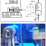 |
Figure 1: The positions of mesh at the electrospinning line
|
To build a pattern we use this condition: The tests perform at concentration 20, 25 and 30 %W/V in voltage 10, 15, 20 and 25 KV with one-layer and 3-layers of mesh and the results investigated.
The technique that we used in this section is “One-factor-at-a-time”. In this technique at first one factor held constant and other experimental factors are varied at a time. In this study at first the voltage held constant (for example 10KV) and the concentration varied(20,25,30%w/v), afterward the concentration held constant and the voltage varied. This method was repeated for all conditions.
The reason that we used 1 layer and 3 layers of mesh is to obtain and observe different patterns and different roughness. The shape of mesh show in fig. 2.
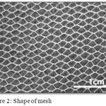 |
Figure 2: shape of mesh
|
Table 1: Sample code, electrospinning parameters and the obtained results
| Sample Code | ||||||||||||||||
| S1 20/10 | S1 25/10 | S1 30/10 | S1 20/15 | S1 25/15 | S1 30/15 | S1 20/20 | S1 25/20 | S1 30/20(c) | S3 30/20(f) | S1 20/25(a) | S1 25/25(b) | S3 25/25(e) | S1 30/25(d) | |||
| Nylon Concentration (%W/V) | 20 | 25 | 30 | 20 | 25 | 30 | 20 | 25 | 30 | 20 | 25 | 30 | ||||
| Electrospinning Voltage (KV) | 10 | 10 | 10 | 15 | 15 | 15 | 20 | 20 | 20 | 25 | 25 | 25 | ||||
| Ra (µm) | – | – | – | – | – | – | – | – | 4.163 | 2.292 | 2.684 | 3.345 | 2.068 | 2.438 | ||
| Rz (µm) | – | – | – | – | – | – | – | – | 18.3 | 12.6 | 14.9 | 17.8 | 12.0 | 13.3 | ||
| Diameter (nm) | – | – | – | – | – | – | – | – | 269 | 253 | 84 | 158 | 138 | 265 | ||
| St Dev | – | – | – | – | – | – | – | – | 60.45 | 64.72 | 18.45 | 35.06 | 18.75 | 57.36 | ||
| Index1=1layer mesh, index3=3layers mesh | ||||||||||||||||
Characterization
The morphology of fibers and surface pattern of samples observed by scanning electron microscopy, JEOL, JSM-840, Japan. Coating of samples is required in the field of electron microscopy to enable or improve the imaging of samples. So, we apply an ultra-thin layer of gold onto specimen for SEM. The name of his method is sputter coating. We used SEM photography in two different magnifications to observe the surface pattern (55X), and the fiber orientation (4500X).
The roughness of surface samples, measured by Mobil Roughness Tester, Mahr, MarSurf PS1, Germany. For the measurement of roughness, MarSurf PS1 portable surface roughness measurement equipment is used. Measuring stylus tip is 2 μm and pressure force is averagely 0.7 mN. Measurement scanning length is adjusted as 17.5mm. MarSurf PS1 portable surface roughness device starts the measurement by moving probe on the sample surface through a 17.5mm length and this device automatically calculates Rz and Ra. Three measurements for each workpiece surface roughness were made and averaged for each test. The results showed in table 1. The shape of roughness tester device and it’s probe show in figure 3.
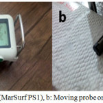 |
Figure 3a: Roughness Tester (MarSurf PS1), b: Moving probe on the sample surface Click here to View figure |
Results
In this study 24 samples (table1) fabricated by “One-factor-at-a-time” technique whit 1 and 3 layers of mesh. At first the voltage held constant and the concentration varied. As a result, at 20KV of voltage and the 30% of concentration the acceptable roughness on the surface created. So, the minimum of voltage was 20KV. Among this 24 samples, only the 6 layers has best web formation and best roughness on their surfaces, so the further experiments were perform on them.
The roughness of these samples measured (Rz and Ra). The formation pattern of Electrospun layers show in Fig. 4. Obviously in this figure can be seen that the samples which 3layers of mesh was used, the pattern did not formation as well as other samples, and also these 2 samples (fig. 4, e&f) has lowest roughness value among all samples, because according to result of roughness test that showed in table 1, the roughness value of sample S3 25/25(e) is 2.065(µm) and the roughness value of sample S3 30/20(f) is 2.292(µm) and maximum roughness is for sample S1 30/20(c) that the roughness value is 4.136(µm).
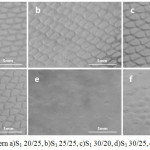 |
Figure 4: Surface pattern a)S1 20/25, b)S1 25/25, c)S1 30/20, d)S1 30/25, e)S3 25/25, f)S3 30/20 Click here to View figure |
Also, according to table 1, the effect of increasing concentration is increase roughness, so that 2.684(µm)for sample S1 20/25(a) to 3.345(µm) for sample S1 25/25(b), and increase voltage lead to decrease roughness, 4.163(µm) for sample S1 30/20(c) to 2.438(µm) for S1 30/25(d).
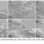 |
Figure 5: SEM images in 55X and 4500X, a)S1 20/25, b)S1 25/25, c)S1 30/20, d)S1 30/25, e)S3 25/25, f)S3 30/20 Click here to View figure |
SEM photography of best 6 samples show in fig. 5. In this picture, we can see the surface pattern (55X) and also the fiber orientation (4500X) of samples. Due to the fig. 5, the best fiber orientation for sample c(S1 30/20). Also in this picture, we can see the surface pattern clearly and we can compare the occupy area of patterns. As it is seen in fig. 5, the sample d(S1 30/25) has a smooth and clear pattern area and this smoot surface lead to obtain lower roughness value in compared with samples a, b and c.
In fig. 6, the diameter of fibers discussed, and the histogram of diameter diagram has been shown. The result of these diagrams are the average of diameter and standard deviation that showed in table 1. According to the result of fig. 6, increasing the concentration of polymer solution lead to increase fiber diameter, from 86nm for sample a(S1 20/25) to 265nm for sample b(S1 25/25). Also increase voltage lead to decrease diameter, from 269nm for sample c(S1 30/20) to 265nm for sample d(S1 30/25).
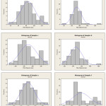 |
Figure 6: Histogram diagram a)S1 20/25, b)S1 25/25, c)S1 30/20, d)S1 30/25, e)S3 25/25, f)S3 30/20 Click here to View figure |
Discussion
The article presented new method for fabrication electrospun nylon 6 layer with different roughness. This significant was obtained by placing a mesh between tip and collector in a conventional electrospinning line. The resulting roughness may use and affect in transdermal systems or a kind of MEMS. The results show that the number of mesh layers or mesh thickness has a negative effect on roughness and lead to decrease roughness, in the other hand increasing concentration lead to increase roughness and increase fiber diameter. Also, increase voltage lead to decrease roughness and fiber diameter. So, according to the obtained results, the best sample is S1 30/20(c). Finally, due to the surface roughness of formation electrospun pattern layers, this layers can be use in drug delivery systems and the produced roughness can be applied for transdermal drug delivery purposes.
Acknowledgements
The authors would like to kindly acknowledge all the supports and funding from Islamic Azad University of Yazd and Standard Research Institute of Iran.
References
- Khajavi, R.; Abbasipour, M. Scientia Iranica. 2012, 19, 2029–2034
CrossRef - Abbasipour, M.; Khajavi, R. Advances in Polymer Technology. 2013, 32
- Marsano, E.; Francis, L.; Giunco, F. Journal of Applied Polymer Science. 2010, 117, 1754–1765
- Sencadas, V.; Correia, D.M.; Areias, A.; Botelho, G.; Fonseca, A.M.; Neves, I.C.; Mendez, S.L. Carbohydrate Polymers. 2012, 87, 1295-1301
CrossRef - Camerlo, A.; Bühlmann-Popa, A.M.; Vebert-Nardin, C.; Rossi, R.M.; Fortunato, G. Journal of Materials Science. 2014, 49, 8154-8162
CrossRef - Wang, B.; Wang, Y.; Yin, T.; Yu, Q. Chemical Engineering Communications. 2010, 197, 1315–1338
CrossRef - Chakraborty, S.; Liao, I.C.; Adler, A.; Leong, K.W. Advanced drug delivery reviews. 2009, 61, 1043-1054
CrossRef - Liu, S.; Zhou, G.; Liu, D.; Xie, Z.; Huang, Y.; Wang, X.; Wu, W.; Jing, X. Journal of Materials Chemistry B. 2013, 1, 101-109
CrossRef - Zamani, M.; Prabhakaran, M.P.; Ramakrishna, S. International journal of nanomedicine. 2013, 8, 2997-3017
- Bazbouz, M.B.; Stylios, G.K. Journal of Applied Polymer Science. 2008, 107, 3023-3032
CrossRef - Gururajan, G.; Sullivan, S.P.; Beebe, T.P.; Chase, D.B.; Rabolt, J.F. Nanoscale. 2011, 3, 3300-3308
CrossRef - Nirmala, R.; Park, H.M.; Navamathavan, R.; Kang, H.S.; El-Newehy, M.H.; Kim, H.Y. Materials Science and Engineering: C, 2011, 31, 486-493
CrossRef - Vaquette, C.; Cooper-White, J.J. Acta biomaterialia. 2011, 7, 2544-2557
CrossRef - Wu, Y.; Dong, Z.; Wilson, S.; Clark, R.L. Polymer. 2010, 51, 3244-3248
CrossRef - Zhang, D.; Chang, J. Nano letters. 2008, 8, 3283-3287
CrossRef - Wang, Y.; Wang, G.; Chen, L.; Li, H.; Yin, T.; Wang, B.; Lee, J.C.; Yu, Q. Biofabrication. 2009, 1, 15001
CrossRef

This work is licensed under a Creative Commons Attribution 4.0 International License.
![]()
A New Edition of Web of Science
Journal Impact Factor
2022: 0.5
Five Year: 0.8
Journal is Indexed in

Cabells Whitelist
![]()


