Study of Structural Properties of Ni3 Pb2 S2 Films
Ho Soonmin
Faculty of Information Technology-Math and Science, INTI International University, Putra Nilai, 71800, Negeri Sembilan, Malaysia.
Corresponding Author E-mail: soonmin.ho@newinti.edu.my
DOI : http://dx.doi.org/10.13005/ojc/330466
In this work, X-ray diffraction technique was applied to determine the structure of nickel lead sulphide thin films prepared by chemical bath deposition. The X-ray diffraction patterns reflect that polycrystalline Ni3Pb2S2 could be obtained using the method explained. The XRD data show that an increasing the deposition time from 7 to 30 hours resulted in increase in the number of peaks.
KEYWORDS:Thin films; solar cell; chemical bath deposition; x-ray diffraction
Download this article as:| Copy the following to cite this article: Soonmin H. Study of Structural Properties of Ni3 Pb2 S2 Films. Orient J Chem 2017;33(4). |
| Copy the following to cite this URL: Soonmin H. Study of Structural Properties of Ni3 Pb2 S2 Films. Orient J Chem 2017;33(4). Available from: http://www.orientjchem.org/?p=35839 |
Introduction
The investigation of the properties of thin films has received great attention all over the world. For example, the obtained films could be characterized by using several techniques such as spectroscopic ellipsometry [1, 2], Raman Spectroscopy [3-5], electrochemical impedance spectroscopy [6-8], profilometer [9, 10], Rutherford backscattering spectrometry [11-14], scanning tunneling microscopy [15-17], and atomic force microscopy [18-20]. These films exhibit excellent chemical, optical, physical and electrical properties. Therefore, these materials are potential candidate for application in laser, sensors, optoelectronic devices, solar cell, photoconductive, electronic devices and thin film transistors.
In this paper, the structure properties of Ni3Pb2S2 films prepared under various deposition times were studied using X-ray diffraction technique. Deposition was carried out in a chemical bath in the presence of complexing agent at room temperature.
Materials and Methods
In this experiment, all the reagents were of analytical grade and de-ionized water (Alpha-Q Millipore) was employed as solvent. The substrates used for the deposition process were indium tin oxide (ITO) coated glass slide. These slides were washed with distilled water, followed by ultrasonic cleaned in acetone solution. During the deposition process, 20 mL of 0.7 M triethanolamine solution (complexing agent) was added into the beaker that contained 25 mL of 0.5 M nickel sulphate and 25 mL of 0.5 M lead nitrate, respectively. Then, 25 mL of 0.5 M of sodium thiosulfate was added into these beakers, respectively. Lastly, these solutions were mixed together for few minutes. The pH of the mixture was adjusted to 1.4 through the addition of a few drops of hydrochloric acid solution. The glass slides were kept vertically in the beaker. The deposition temperature was room temperature and the deposition time varied between 7-30 hours. After the deposition, these films were washed with distilled water and dried in air.
The structure of the films was studied by X-ray diffraction (XRD) with a PANalytical X-Pert PW 3040 diffractometer equipped with a CuKα (λ=0.15418 nm) radiation source. Data were collected by step scanning from 10° to 90° with a step size of 0.026° (2θ).
Results and Discussion
The X-ray diffraction (XRD) is mostly used in scientific industries, material science and engineering fields for the measurement of compounds. X-ray diffraction has many advantages such as the cheapest technique, x-rays are not absorbed very much by air and the samples need not be in an evacuated chamber. Therefore, this technique was used to investigate the structure of samples by many researchers [21-25]. Figures 1-4 show the films were synthesized for different deposition times. The XRD patterns display that these films are polycrystalline with rhombohedral structure.
Figure 1 shows the XRD pattern for the films deposited for 7 hours at room temperature. Identification of the peaks such as (012) and (110) on the X-ray diffraction pattern indicates that less materials could be deposited onto substrates in shorter deposition time. These peaks were in good agreement with the Joint Committee on Powder Diffraction Standard (JCPDS) data (Reference code: 00-006-0459) belonging to the Ni3Pb2S2. Also, XRD pattern displays that the intensities of the signals are rather weak if compared to other samples due to the thin film nature of the samples.
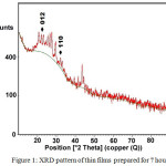 |
Figure 1: XRD pattern of thin films prepared for 7 hours |
Figure 2 and Figure 3 show the XRD patterns for the films prepared for 9 hours and 26 hours, respectively. In these cases, there are three peaks corresponding to the (110), (024) and (300) planes have been observed in both samples. However, comparison between these samples indicates that the intensity of the peaks increased for the films prepared for 26 hours. The observed d-values and standard d-values are shown in Table 1.
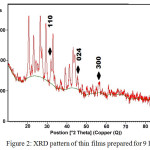 |
Figure 2: XRD pattern of thin films prepared for 9 hours |
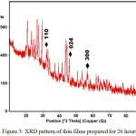 |
Figure 3: XRD pattern of thin films prepared for 26 hours |
Table 1: Comparison between observed d-values of Ni3Pb2S2 thin films prepared at different deposition times with JCPDS data.
|
Deposition time (h) |
Standard d-values (Å) |
Observed d-values (Å) |
Plane (hkl) |
|
7 |
3.97 |
3.86 |
12 |
|
2.8 |
2.78 |
110 |
|
|
9 |
2.8 |
2.81 |
110 |
|
1.97 |
2 |
24 |
|
|
1.61 |
1.62 |
300 |
|
|
26 |
2.8 |
2.78 |
110 |
|
1.97 |
1.96 |
24 |
|
|
1.61 |
1.61 |
300 |
|
|
30 |
3.97 |
3.83 |
12 |
|
2.8 |
2.78 |
110 |
|
|
1.97 |
1.98 |
24 |
|
|
1.61 |
1.63 |
300 |
|
|
1.39 |
1.4 |
220 |
Figure 4 shows the XRD pattern for the films prepared for 30 hours. The results are well matched with the JCPDS values for Ni3Pb2S2. When the deposition time was increased to 30 hours, the intensity and the number of the peaks were increased. The XRD pattern reflects that the (012), (110), (024), (300) and (220) planes have been deposited.
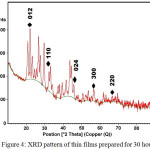 |
Figure 4: XRD pattern of thin films prepared for 30 hours |
Conclusion
The effect of deposition time on nickel lead sulphide thin films prepared by chemical bath deposition was investigated in this work. X-ray diffraction pattern shows that increasing the deposition time from 7 to 30 hours resulted in increase in the number of peaks and intensity of the Ni3Pb2S2 peaks.
Acknowledgement
This research work was supported by INTI International University under INTI Research Grant 2015(2): INT-FOSTEM-01-02-2015.
References
- Yim, C.M.; O’Brien, N.; McEvoy, S.; Winters, I.; Mirza, J.; Lunney, J. J. Appl. Phys. Lett. 2014, 104, DOI: http://dx.doi.org/10.1063/1.4868108.
- Shaaban, E.R.; Emam, M.; Abbady, G.; Prakash, D.; El-Hagary, M.; Afify, N.; Verma, K.D. Solid State Sci. 2015, 52, 65-71.
- Xi, Y.; Bouanani, L.E.; Xu, Z.; Manuel, A.Q.; Majid, M. J. Mater. Chem.2015, 3, 9781-9788.
- Prasad, M.;Thyagarajan, K.; Kumar, B.R.IOP Conf. Series: Mater. Sci. Eng.2016, doi:10.1088/1757-899X/149/1/012051.
- Kathalingam, A.; Mahalingam, T.; Sanjeeviraja, C. Mater. Chem. Phys. 2007, 106, 215-221.
- Tlig, F.; Gannouni, M.; Assaker, I.B.; Chtourou, R. J. Photochem. Photobiol. A: Chem.2017, 335, 26-35.
- Ibtissem, B.A.; Mounir, G.; Amina, L.; Radhouane, C.Superlattices and Microst.2014, 75, 159-170.
- Atanu, J.; Prasenjit, H.; Mukul, H.; Jayati, D. Mater. Chem. Phys. 2016, 183, 173-180.
- Khallaf, H.; Oladeji, I.O.; Chow, L. Thin Solid Films2008, 516, 5967-5973.
- Ayeshamariam, A.; Kashif, M.; Raja, S.M.; Jagadeswari, S.; Saravanankumar, D.; Alhaji, N.M.I.; Mohideen, A.U.; Bououdina, M.; Jayachandran, M.Int. J. Emerging Technol. Adv. Eng. 2014, 4, 584-590.
- Abiodun, E.A.; Emmanuel, A.; Bidini, A.T.; Fassasi, A.Y.J. Mater. 2015,http://dx.doi.org/10.1155/2015/215210.
- Ho, S.M.Eur. J. Sci. Res.2016, 142, 343-349.
- Dahbi, N.; Arafah, D. Energy Proc. 2012, 18, 85-90.
- Alarcon-diez, V.; Eddrief, M.; Vickridge, I.Nucl. Instrum. Meth B2016, 371, 224-229.
- Lin, K.C.; Li, Y.S.; Shen, Y.T.; Wu, M.K.; Chi, C.C. Phys. C: Superconductivity2013, 495, 74-78.
- Pamela, P.M.; Joseph, L.; Angus, R. Surf. Sci.2015, 636, 8-12.
- Soumyo, C.; Amlan, J.P. Sol. Energy Mater. Sol. Cells2017, 160, 233-240.
- Ho, S.M.; Tee, W.T.; Lim, K.S.; Anuar, K.; Saravanan, N. Res. J. Appl. Sci. Eng. Technol. 2011, 3, 513-518.
- Ho, S.M. Oriental J. Chem.2016, 32, 1515-1519.
- Anuar, K.; Saravanan, N.; Ho, S.M.; Atan, S.Stud. U. Babes-Bolyai Chem. 2010, 55, 5-11.
- Sandeep, G.; Pathak, R.K. Oriental J. Chem. 2013, 29, 1469-1474.
- Anuar, K.; Ho, S.M.; Tan, W.T.; Abdul, H.A.; Saravanan, N. Macedonian J. Chem. Chem. Eng. 2010, 29, 97-103.
- Nathera, A.A.A. Int. J. Nanoelectron Mater. 2013, 6, 17-28.
- Saravanan, N.; Ho, S.M.; Anuar, K. Turk. J. Sci. Technol.2011, 6, 17-23.
- Abbas, T.; Slewa, L. Int. J. Nanoelectron Mater. 2015, 8, 111-120.

This work is licensed under a Creative Commons Attribution 4.0 International License.
![]()
A New Edition of Web of Science
Journal Impact Factor
2022: 0.5
Five Year: 0.8
Journal is Indexed in

Cabells Whitelist
![]()


