Co-Sensitized Tio2 Photoelectrodes by Multiple Semiconductors (Pbs/Pb0.05cd0.95s/Cds) to Enhance the Performance of A Solar Cell
Supriyono1,2, Ahmad Zakaria1, Yuni Krisyuningsih Krisnandi2 and Jarnuzi Gunlazuardi2
1Department of Chemical Analysis, Politeknik AKA Bogor,Bogor 16154, Indonesia.
2Department of Chemistry, Faculty of Mathematics and Sciences,Universitas Indonesia, Depok 16424, Indonesia.
Corresponding Author E-mail: supriyono272@gmail.com
DOI : http://dx.doi.org/10.13005/ojc/330515
The effect of PbS/Pb0.05Cd0.95S/CdS co-sensitization on the quantum dot-sensitized solar cell performance have been investigated. In this research, a TiO2 nanoparticles was prepared by a sol gel method and immobilized to the FTO (fluorine tin oxide) substrate by dip coating technique. The formation of PbS, Pb0.05Cd0.95S, and CdS quantum dots (QDs) sensitized TiO2 photoelectrode was carried out by successive ionic layer adsorption and reaction (SILAR) method. The as-prepared materials were characterized by scanning electron microscopy, energy dispersive spectroscopy, X-ray diffraction, and X-ray photoelectron spectroscopy. Our photoelectrochemical evaluation indicated that the photocurrent of PbS/Pb0.05Cd0.95S/CdS multiple semiconductor (0.363 mA/cm2) is higher than the CdS single sensitizer (0.190 mA/cm2), resulting an increase in a photocurrent of 91%. Under 3.5 mW/cm2 illumination, we found that this photoelectrodes have an optimum short-circuit photocurrent density (Isc) of 0.429 mA/cm2 and energy conversion efficiency of 1.42%, which is 160% higher than that of a CdS single sensitizer (0.54%). The excellent photoelectrochemical properties of our photoanode, suggest that the TiO2 films co-sensitized by PbS/Pb0.05Cd0.95S/CdS quantum dots have potential application in a solar cells.
KEYWORDS:solar cell; quantum dots; SILAR method; co-sensitization
Download this article as:| Copy the following to cite this article: Supriyono S, Zakaria A, Krisnandi Y. K, Gunlazuardi J. Co-Sensitized Tio2 Photoelectrodes by Multiple Semiconductors (Pbs/Pb0.05cd0.95s/Cds) to Enhance the Performance of A Solar Cell. Orient J Chem 2017;33(5). |
| Copy the following to cite this URL: Supriyono S, Zakaria A, Krisnandi Y. K, Gunlazuardi J. Co-Sensitized Tio2 Photoelectrodes by Multiple Semiconductors (Pbs/Pb0.05cd0.95s/Cds) to Enhance the Performance of A Solar Cell. Orient J Chem 2017;33(5). Available from: http://www.orientjchem.org/?p=38502 |
Introduction
Increasing demand for energy is forcing us to seek into an alternative new resources. Among many available candidates, solar energy is ideal to meet the target because of its abundant, clean, and inexhaustible characteristics. Recently, quantum dot-sensitized solar cells (QDSSCs) have received much attention for alternative of dye-sensitized solar cells (DSSCs) owing to their band gap tune ability, higher absorption coefficient of quantum dots compared to dye molecules, and the ability of multiple-carrier generation1-4. However, the efficiency of QDSSCs is lower compared with other type DSSCs, which restricts their potential application. Thus it is still a crucial issue to enhance its efficiency. A typical QDSSC, just like DSSC, consists of a QDs-sensitized TiO2 film photoanode, a redox electrolyte, and a platinized counter electrode5,6. As an important component, the photoanode plays a role in the separation of photogenerated charge carriers and the transportation of electrons. TiO2 films have been demonstrated to be promising candidate as photoanodes due to their appropriate energy band position and both thermal and chemical stability in solution. However, the large band gap of TiO2 (3.2 eV) limits its absorption only to the ultraviolet region, which takes only 3 – 5% of the whole solar spectrum reaches earth surfaces.
To improve the performance of QDSSCs, various nanostructures have been employed to fabricate the photoanodes, such as mesoporous films7–9, hierarchical sphere10, nanowires (NWs), nanorods (NRs) and nanotubes (NTs) arrays. Recently, many new strategies, especially the surface and interface treatment, were also employed to modify the nanostructures of the photoanodes, aiming to reduce the recombination and improve the transport of the photo-excited carriers at the interface10. To extend the activity of a photoelectrode into the visible light region, various approaches were employed including doping TiO2 with other impurities, using dye-sensitized solar cells (DSSCs), and very recently using the composite semiconductors such as QDs-sensitized solar cells (QDSCs)11-13.
Many kinds of small band gap semiconductors that can absorb light in the visible region, e.g., CdS13, PbSe14, CdSe15, InP16, and CdTe17, have been used as sensitizers. Among them, CdS is semiconductor with direct band gap (Egap) of 2.25 eV, which means CdS can trigger wider light absorption range compared to TiO2. However, to accelerate charge separation in bulk/single crystal material, the level of the conduction band (CB) edge which provides the electron injection driving force from QDs to TiO2 should be taken into account. It is known that CdS has a high CB edges with respect to that of TiO2, and a higher electron injection efficiency of CdS was found18. PbS is also fascinating sensitizer for QDSSC. The bulk band gap of PbS (0.41 eV) can be easily manipulated by changing the particle size. The poor stability of PbS quantum dots is a major drawback for QDSSC application. Thus in order to solve the problem, CdS shells are coated on the PbS sensitizer to prevent the corrosion by the polysulfide electrolyte and suppress the recombination at the semiconductor/electrolyte interface19-21. Different from the dye molecules, quantum dot sensitizers may have defects or dislocation. Therefore, enhancing the quality of the quantum dots is an important issue for optimizing QDSSCs22.
In this study, we prepared TiO2 photoanode sensitized by multiple semiconductors, which include PbS, Pb0.05Cd0.95S, CdS and assembled it into a typical QDSSC. The effect of adding a layer of quantum dot / sensitizer to the value of the photocurrent and efficiency of the solar cells, then was investigated and will be discussed herein.
Materials and Methods
Materials
All chemicals and solvents used in this study were of reagent grade. Titanium (IV) isopropoxide, polyethylene glycol (Mr = 1000), triethanolamine, H2PtCl6, sulphur were purchased from Sigma Aldrich. While methanol, ethanol, 2-propanol, Cd(CH3COO)2.2H2O, Na2S.9H2O, Pb(NO3)2, KCl were purchased from Merck. Distilled water produced from a BioPure purification system was used throughout the experiments and homemade FTO (75X25X1,4 mm3, sheet resistance = 21Ω/sq) were made by spray pyrolysis method23.
Instrumentation
XRD patterns of the prepared film were conducted on X-ray Diffractometer XRD 7000 Shimadzu Cu Ka radiation (l= 0.15418 nm) that operated at 40 kV and 30 mA. FESEM images were taken using FESEM (FEI-Inspect F50). The percentage of elemental composition in the composite film was obtained from energy dispersive spectroscopy (EDS Apollo X). The oxidation state of titanium, cadmium, lead, sulfur, and platinum were examined using Thermo VG Scientific-Sigma Probe X-ray photoelectron spectroscopy (XPS) with mono-chromated Al Kα radiation and operating pressure in the sampling chamber was below 5 × 10⁻⁹ Torr. Photocurrent was measured by electrochemical workstation with a three-electrode configuration, which was connected to a computer-controlled potentiostat (e-DAQ/e-recorder 401) to record the generated photocurrent. TiO2 photoanode was placed as working electrode, while a Pt wire and Ag/AgCl was placed as counter and reference electrode, respectively. The supporting electrolyte was Na2S 0.1M. As source of visible irradiation is 60W wolfram lamp with the intensity 2.20 mW/cm2. Solar cells performance evaluation was measured by Edaq potensiostat connected with e-recorder 401.
Procedure
Preparation of FTO/TiO2 film24
Titanium tetraisopropoxide (TTIP), polyethylene glycol (PEG, Mr = 1000), triethanolamine, ethanol, FTO (fluorine tin oxide) and distilled water were used in this experiment. TiO2 sol was prepared by mixing of 7.5 mL TTIP, 2.4 mL triethanolamine, and 36 mL of ethanol. The mixture was stirred with a magnetic stirrer at room temperature for 1.5 hours, then was added by adequate ethanol-water (4.5:0.5) and 2 grams of PEG, and stirred with a magnetic stirrer for 1.5 hours. The resulting sol then was used to coat the FTO glass by a dip coating method, and then annealed at 500ºC for 1 hour. This step was repeated 5 times to obtain TiO2 film on the FTO surface (FTO/TiO2).
Preparation of FTO/TiO2/CdS Film
CdS quantum dot (QD) was prepared by a SILAR (successive ionic layer adsorption and reaction) method. Individual solution containing Cd(CH3COO)2 and Na2S were used as a Cd and S precursor to obtain CdS quantum dot. The CdS was deposited directly by immersing the FTO/TiO2 glass into an aqueous solution of Cd(CH3COO)2 0.3M for 2 minutes, then rinsed with distilled water. Then was immersed in aqueous solution of Na2S 0.1M for 2 minutes, then rinsed with distilled water. This step was repeated 10 times until the optimum CdS layer was formed. The CdS layer on FTO/TiO2 surface then was dried at room temperature for few minute to obtain FTO/TiO2/CdS film.
Preparation of FTO/TiO2/PbS/CdS Film
PbS was prepared by a SILAR (successive ionic layer adsorption and reaction) method. The FTO/TiO2 was soaked in the solution of Pb(NO3)2 0,02M in methanol for 2 minutes and then rinsed with ethanol. Then was soaked in a solution of Na2S 0,01M in methanol: water (1:1) for 5 minutes, then rinsed with ethanol. This step was performed up to three cycles in order to obtain desired thickness. Then proceed with the CdS layer in the same manner as above. The FTO/TiO2/PbS film was immersed into an aqueous solution of Cd(CH3COO)2 0.3M for 2 minutes, then rinsed with distilled water. Then was immersed in aqueous solution of 0.1M Na2S for 2 minutes, then rinsed with distilled water. This step was repeated 10 times until the optimum CdS layer was formed. The CdS layer on FTO/TiO2/PbS surface then was dried at room temperature for few minute to obtain FTO/TiO2/PbS/CdS film.
Preparation of FTO/TiO2/PbS/ Pb0.05Cd0.95S /CdS Film
The FTO/TiO2 was soaked in the solution of Pb(NO3)2 0,02M in methanol for 2 minutes and then rinsed with ethanol. Then was further soaked in a solution of Na2S 0,01M in methanol : water (1:1) for 5 minutes, then rinsed with ethanol. These steps were done in three repeating cycles in order to obtain desired thickness. Then proceed with the Pb0.05Cd0.95S layer using SILAR method. First, a solution of Pb/Cd 0,02M in methanol (with a molar ratio of Pb/Cd = 5/95) was prepared by mixing a solution of Pb(NO3)2 and Cd(CH3COO)2 24. QD deposition was performed with SILAR method, firstly it was soaked in a solution of Pb/Cd 0,02M for 2 minutes, then rinsed with ethanol. Then it was soaked in a solution of Na2S 0,01M for 5 minutes, then rinsed with ethanol. This step was performed up to three cycles in order to obtain the desired thickness. Then it was proceed with the CdS layer in the same manner as above to obtain FTO/TiO2/PbS/Pb0.05Cd0.95S/CdS film
Characterization
Characterization of the film structure was done by using X-ray diffractometer (Shimadzu XRD 7000) with CuKα radiation (λ = 1.5418 Å), at 30 kV, 10 mA. Film thickness and morphology of the film surface was observed with FESEM (FEI-Inspect F50). The composition of the constituent elements measured by Energy Dispersive Spectroscopy (Apollo X). The oxidation states of constituent elements were examined by X-ray photoelectron spectroscopy. Photocurrent response was measured using an electrochemical workstation (e-DAQ/e-recorder 401) using 60W wolfram lamp as visible light source. Ag/AgCl electrode was used as a reference electrode, while platinum (Pt) was used as a counter electrode and Na2S 0,1M as an electrolyte. Photocurrent measurements using multipulse amperometry with a potential = 0 volts and scan time = 100 second.
Performance Evaluation
Performance evaluation was done by using Edaq potensiostat connected with e-recorder 401. TiO2 photoanode was placed as a solar cell working electrode and FTO/Pt was placed as counter electrode. Redox couples Na2S 0.2M, S 1M, KCl 0.02M solution was used as an electrolyte and 150W halogen lamp (3.50 mW/cm2 was measured by lux meter) was used as irradiation sources. Isc (short circuit current), and Voc (open circuit voltage) was measured by linear sweep voltammetry (LSV) with scan rate of 40 mV/s from 500 mV to 0 mV under visible illumination.
After solar cells have been fabricated, it should be evaluated for a number of parameters which provide its performance information. These include Isc (short circuit current, mA/cm2), Voc (open circuit voltage, mV), FF (fill-factor) and h (power conversion efficiency). Based on I–V curve, the fill factor (FF) is defined as :
where Im (mA/cm2) and Vm (mV) are the photocurrent and photovoltage for maximum power output (Pm, mW/cm2), The overall energy conversion efficiency (h) is defined as:
Results and Discussion
Preparation and characterization of the nanostructured TiO2 photoanode
Composition and crystal structure of the nanostructured TiO2 photoanode
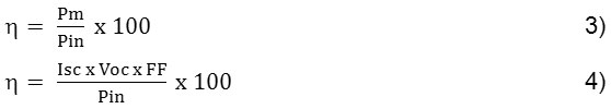
Based on patterns of X-ray diffraction in figure 1.a, it appears that FTO has a value of 2θ = 26.4º, 33.7º, 37.7º, 51.6º, 54.4º, 61.6º, 64.8º and 65.7º with the indexes Miller (110), (101), (200), (211), (220), (310), (112), and (301). This shows that according to JCPDS 41-1445, our FTO has cassiterite structure . After FTO coated with TiO2, it appears the new peaks at 25.3º and 47.9º and the other peak with increased intensity in 37.8º (figure 1.b). This corresponds to JCPDS 21-1272, thus it can be concluded that our TiO2 has crystallite structure of anatase.
The anatase crystallite size of TiO2 was estimated using the Scherrer equation.

where the constant k is a shape factor usually ∼0.9, λ is the wave length of X-ray (0.15418 nm), β is the FWHM in radians and θ is the Bragg’s angle.
The estimation shows that the mean crystallyte size of the anatase TiO2 individual particles calculated from Eq. (5) is 22–50 nm. While the dominant peak of rutile TiO2 at 27.4º, 36.1º and 54.3º (JCPDS 21-1276) are not visible at all.
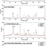 |
Figure 1 : X-ray diffraction patterns of TiO2 nanostructured photoanode |
From XPS spectra, useful information was obtained to assign the complete chemical composition of the sample surface. The survey spectrum in figure 2.a gives XPS profile of the as-synthesized TiO2 nanoparticles.
 |
Figure 2 : XPS spectrum of FTO/TiO2 thin film |
The constituents peaks were identified to be titanium (Ti), oxygen (O) and carbon (C). The X-ray photoelectron spectroscopy (XPS) spectra were analyzed for the TiO2 film in order to study the surface composition of the TiO2 thin film. The Ti2p3/2 and Ti2p1/2 spin-orbital splitting photoelectrons for TiO2 (figure 2.b) are located at binding energies of 458.7 and 464.5 eV, respectively, which is consistent with the values of Ti4+ in the TiO2 lattices, as observed earlier by Hung, et al.25. According to the literature, the Ti2p3/2 binding energy of TiO2 is in the range of 458.7–459.2 eV, while the binding energy of titanium in the oxidation state 3+ is in the range of 456.2–457.4 eV26. Therefore, titanium exists on the surface in the form of TiO2 with oxidation state 4+. The photoelectron spectra of O1s can be deconvoluted into two peaks (figure 2.c). The O1s main peak at 529.9 eV is assigned to the metallic oxides, which is consistent with the binding energy of O2- in the TiO2 lattices. A shoulder to the main O1s peak can be observed at high binding energy, 531.8 eV which can be attributed to the hydroxyl groups or chemisorbed water molecules adsorbed on TiO2 surface. In addition, it also shows the presence of C peak (figure 2.d) at 285.1, 286.8 and 288.6 eV. The deconvolution of the C1s peaks indicates the presence of two peaks at 286.3 and 288.8 eV other than the main peak of sp2-carbon at 284.6 eV. The peaks at 286.3 and 288.8 eV can be attributed to hydroxyl carbon (C–OH) and carboxyl carbon (O=C–O), respectively27. This indicates that there are more carbon-containing residues on the films. This residues were suspected from uncompleted combustion of PEG molecules during calcination.
After CdS deposited on the surface of TiO2, it appears a different X-ray diffraction patterns. In the figure 1.c, it appears that the peak 26.4º and 51.6º increased in intensity and appears a small peak at 47.4º. This shows that the CdS has successfully synthesized by SILAR method and according to JCPDS 10-0454, this CdS has hawleyite crystallite structure. The small intensity of CdS peaks was caused by a small quantities of CdS deposited on the TiO2 surface. It was only about 1: 6 (Cd: Ti), as shown in the EDS spectrum in figure 3.b. According to Balaz, et al.28, CdS has two structures, these are hexagonal α-CdS called greenockite (JCPDS 41-1049) and cubic β-CdS called hawleyite (JCPDS 10-0454). Our CdS is in accordance with the hawleyite structure. Besides coated by CdS, TiO2 is also coated by PbS. Characterization of FTO/TiO2/PbS/Pb0.05Cd0.95S/CdS layer with X-ray diffraction does not show any clear PbS peaks. Only a small peak seen in 53.4º (figure 1.d), this due to the amount of PbS deposited on the TiO2 surface is very small, only about 1:12 (Pb: Ti) as shown in the EDS spectrum in figure 3.c. Beside that reason, PbS and CdS layer is only dried at room temperature without any calcination, so likely PbS and CdS still have an amorphous structure and the resulted peak tends to be broaden. PbS has only a galena single crystal structure, so it can be ascertained that our PbS has galena structure (JCPDS 05-0592).
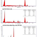 |
Figure 3 : EDS spectrum and elemental composition of TiO2 nanostructured photoanode |
The spectrum of the overall survey scan of FTO/TiO2/PbS/Pb0.05Cd0.95S/CdS thin layer (figure 4.a) indicates the presence of Ti, O, Pb, Cd, and S in the sample. The Cd3d5/2 and Cd3d3/2 binding energies are equal to 405.0 eV and 411.8 eV (figure 4.b) and it corresponds to Cd2+.
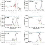 |
Figure 4 : XPS spectrum of FTO/TiO2/PbS/Pb0.05Cd0.95S/CdS thin films |
For cadmium sulfide, the Cd3d5/2 binding energy is in the range of 404.4 – 405.7 eV29. Figure 4.d shows XPS spectra of S2p levels of CdS nanoparticles. S2p peaks observed at 161.3 eV (for S2p3/2) and 162.7 eV (for S2p1/2) are attributed to metal sulfide. Observed values of the S2p3/2 binding energy for sulfur in the sulfides is in the range of 161.1–161.7 eV29; sulfates and sulfites are characterized by the higher S2p binding energy in the range of 168–170 eV30. The resolution of the XPS spectra of the Pb resulted in peaks at different binding energies. The Pb4f7/2 and Pb4f5/2 spin-orbital splitting photoelectrons for PbS (figure 4.c) are located at binding energies of 138.2 eV and 142.9 eV, respectively, which is consistent with the values of Pb2+ in the PbS lattices31. In addition, it also shows the presence of C peak (figure 4.e) as well as O peak (figure 4.f) at 285.0 and 530.0 eV, respectively, as impurities. The O1s main peak at 530.0 eV is assigned to the metallic oxides, which is consistent with the binding energy of O2- in the TiO2 lattices. A shoulder to the main O1s peak can be observed at higher binding energy, 532.0 eV which can be attributed to the hydroxyl groups or chemisorbed water molecules adsorbed on TiO2 surface. The deconvolution of the C1s peaks indicates the presence of two peaks at 286.3 and 288.8 eV other than the main peak of sp2-carbon at 284.6 eV. The peaks at 286.3 and 288.8 eV can be attributed to hydroxyl carbon (C–OH) and carboxyl carbon (O=C–O), respectively. This peaks were suspected from uncompleted evaporation of methanol / ethanol solvent used in Pb2+ and S2- solution.
Surface morphology of the nanostructured TiO2 photoanode
From figure 5.a shows that the TiO2 deposited on the surface of the FTO, has a porous structure with a diameter of less than 1 µm. Pores are from PEG template that lost during calcination. Pores are useful to hold sensitizer in larger quantities. CdS and PbS will fill the pores of TiO2 so that these pores will be full after the sensitizer enter into it, as shown in figure 5.b and 5.c. But in wide pores, sensitizer only able to coat the inner walls of the pores so that the pores are still open with a smaller diameter (figure 5.c). PbS and CdS largely occupy space in the pores and only a few of this sensitizer which occupies on the surface of TiO2. This reason is supported by a cross-sectional images in figure 6, that the thickness of TiO2/PbS/Pb0.05Cd0.95S/CdS layer is only slightly thicker than the TiO2 layer.
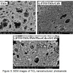 |
Figure 5 : SEM images of TiO2 nanostructured photoanode |
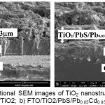 |
Figure 6 : Cross-sectional SEM images of TiO2 nanostructured photoanode a) FTO/TiO2; b) FTO/TiO2/PbS/Pb0.05Cd0.95S/CdS |
Photoelectrochemical response of the nanostructured TiO2 photoanode
Light absorption, particularly in the visible region, can be increased by using a narrow bandgap quantum dots. Two or more different band gap quantum dots can be used at a same time so that the light is not absorbed by the first quantum dot, can still be absorbed by the second quantum dot. This phenomenon is called as co-sensitization, the sensitization was carried out by two or more sensitizers. With the co-sensitization makes the larger absorption of the incident light. The more light is absorbed, the more likely the resulting photocurrent. In this study two sensitizers, CdS and PbS were used. CdS has a bandgap 2.25 eV coupled with PbS which has a band gap of 0.41 eV. CdS has absorption in the visible region is at a wavelength of 550 nm while PbS has absorption in the infra red region (+ 3000nm). With the merger of two quantum dot, it is expected to increase the absorption of visible light so that it will increase its photocurrent. From the observation of the photocurrent in figure 7, it is clear that the two sensitizer PbS and CdS able to improve the higher photocurrent .
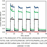 |
Figure 7 : The photocurrent of TiO2 nanostructured photoanode A)FTO/TiO2, B)FTO/TiO2 /CdS, C)FTO/TiO2/PbS/CdS, D)FTO/TiO2/PbS/Pb0.05Cd0.95S/CdS (illuminated with 60W wolfram lamp, 2.20 mW/cm2; electrolyte = Na2S 0.1M, bias potensial = 0 Volt) |
Mixture of PbS and CdS, is Pb0.05Cd0.95S which has a bandgap between them, was able to increase the absorption in the visible region and simultaneously improve its photocurrent. FTO/TiO2/CdS layer generates a photocurrent of about 0.190 mA/cm2 while FTO/TiO2/PbS/CdS about 0.302 mA/cm2, so that the PbS able to increase the photocurrent of 59%. The existence of Pb0.05Cd(0.95S layer between PbS and CdS layer is useful to accelerate the transfer of electrons from CdS layer to PbS. FTO/TiO2/PbS/ Pb0.05Cd0.95S /CdS layer able to generate photocurrent up to 0.363 mA/cm2. Therefore, combination of PbS and Pb0.05Cd0.95S layer able to increase the photocurrent up to 91%.
The mechanism of electron flow is highly dependent on the position of the conduction band of each semiconductor. CdS semiconductor which has a conduction band edge of -4.0 eV is estimated as the beginning of a flow of electrons. CdS with the band gap 2,25eV will be excited when exposed by the light with a wavelength smaller than 550 nm. From the CdS conduction band, the electrons will flow into the conduction band PbS of -4.1 eV. In addition to receive an electrons from CdS, PbS semiconductor can also be a source of electrons. PbS with a band gap of 0.41 eV will be excited when exposed by the light with a wavelength of less than 3000 nm. Electrons from the PbS valence band will move toward the PbS conduction band. Furthermore, from the PbS conduction band, electrons proceed to the TiO2 conduction band of -4.2 eV. From the TiO2 conduction band, the electrons move toward the SnO2 conduction band of -4.8 eV, to get to the external circuit. Meanwhile, to prevent electron-hole recombination is required hole transporting material is S2- from the redox electrolyte. For more details of the electrons flow, can be seen in figure 8 below.
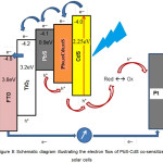 |
Figure 8 : Schematic diagram illustrating the electron flow of PbS-CdS co-sensitized solar cells |
Preparation of Pt counter electrode
Pt counter electrode is made by depositing Pt on the surface of the FTO. From X-ray diffraction pattern in figure 9, it appears that the metals Pt have been successfully deposited on the surface of the FTO.
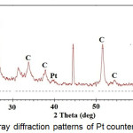 |
Figure 9 : X-ray diffraction patterns of Pt counter electrode |
It appears from the new peak appearing at 39,4º and 66.4º which is the peak of platinum according to JCPDS 88-2343. The amount of Pt deposited on the surface of the FTO is very small that is around 1:10 (Pt: Sn) as shown in the EDS spectra in figure 10, so that the resulted peak in X-ray diffraction pattern has also a small intensity. Although the amount of Pt is very small but platinum crystals have a uniform shape, as shown in figure 11.
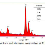 |
Figure 10 : EDS spectrum and elemental composition of Pt counter electrode |
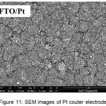 |
Figure 11: SEM images of Pt couter electrode |
Figure 12.a is the typical survey spectrum of FTO/Pt thin film, showing the presence of Pt, Sn, O and C. The corresponding Pt4f spectra are shown in figure 12.b. It is seen that the Pt4f7/2 binding energy is 70.7 eV that is typical of metallic platinum. According to Kalinkin, et al.32, for the chloride complexes, the Pt4f spectrum is shifted to higher binding energies by a value proportional to the oxidation state of platinum. For example, for K2PtCl4 (the oxidation state of platinum is Pt2+) and K2PtCl6 (Pt4+), the binding energy (Pt4f7/2) values are 73.1 eV and 75.2 eV, respectively. As a consequence, the shift of the Pt4f7/2 photoemission line with respect to that of the metal is 2.0 eV for Pt2+ and 4.1 eV for Pt4+, i.e. about 1 eV per unit oxidation number. Binding energies of Sn3d3/2 and Sn3d5/2 electrons in the surface layer of the FTO materials were found to be 494.9 eV and 486.7 eV respectively, which corresponded to Sn4+ in the tin dioxide
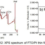 |
Figure 12 : XPS spectrum of FTO/Pt thin film |
Performance evaluation of the solar cells
Solar cells was constructed by assembling the working electrode and the counter electrode by using a redox electrolyte Na2S/S. Solar cell performance evaluation was done by using the potentiostat and 150W halogen lamp as a light visible source. Intensity of halogen lamp was measured by a lux meter and was obtained the intensity at a distance of 10 cm of 3.50 mW/cm2. From 3 different configurations are FTO/TiO2/CdS, FTO/TiO2/PbS/CdS, FTO/TiO2/PbS/ Pb0.05Cd0.95S/CdS obtained I-V curves as indicated in figure 13.
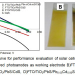 |
Figure 13 : Left : I-V curve for performance evaluation of solar cells; Right : Color of TiO2 nanostructured photoanodes as working electrode B)FTO/TiO2/CdS, C)FTO/TiO2/PbS/CdS, D)FTO/TiO2/PbS/Pb0.05Cd0.95S/CdS |
Based on the I-V curve in figure 13, it can be determined the value of the fill factor, Isc, Voc, and efficiency, using the formula described above, in order to obtain the following results, as indicated in table 1.
Table 1: The value of the fill factor, Isc, Voc, and efficiency of solar cells
|
Sensitizer |
Imax |
Vmax |
Isc |
Voc |
FF |
Pmax |
Pin |
h |
|
mA/ cm2 |
mV |
mA/ cm2 |
mV |
mW/ cm2 |
mW/ cm2 |
(%) |
||
|
CdS |
0.1172 |
162 |
0.2298 |
327 |
0.253 |
0.0190 |
3.501 |
0.54 |
|
PbS/CdS |
0.1462 |
257 |
0.2446 |
469 |
0.328 |
0.0376 |
3.501 |
1.07 |
|
PbS/Pb0.05 Cd0.95S/CdS |
0.2285 |
217 |
0.4286 |
452 |
0.256 |
0.0496 |
3.501 |
1.42 |
From the table 1, it is obtained the efficiency for CdS single sensitizer = 0:54% and using (PbS+CdS+Pb0.05Cd0.95S) = 1.42%. Thus an increase in efficiency of around 160% on solar cells using multiple semiconductor compared with solar cells using a single semiconductor of CdS.
Conclusion
Based on the results obtained, it can be concluded that TiO2 nanostructured photoanode have been successfully prepared by utilizing two semiconductor namely CdS and PbS. Quantum dot of CdS, PbS and Pb0.05Cd0.95S have been successfully prepared using SILAR method and obtained photocurrent of 0.190 mA/cm2 for configuration FTO/TiO2/CdS, 0.302 mA/cm2 for FTO/TiO2/PbS/CdS and 0.363 mA/cm2 for FTO/TiO2/PbS/Pb0.05Cd0.95S/CdS. Sensitizers which use multiple semiconductors namely PbS, CdS and Pb0.05Cd0.95S able to increase the photocurrent of 91% greater than that using a single semiconductor of CdS. Based on the incident light of 3.5 mW/cm2,the all three types constructed solar cells show efficiency of 0.54%, 1.07% and 1.42%, respectively. It can be concluded that the efficiency has been increase of around 160% when multiple semiconductors PbS, CdS, Pb0.05Cd0.95S were used.
Acknowledgements
One of the authors (Supriyono) wish to thank to Industrial Education and Training Center, Ministry of Industry of Indonesia for providing the research funding. Partial support from Research Cluster Scheme Universitas Indonesia, and opportunity provided by KAIST (Korean Advanced Institute of Science and Technology) for SEM and XPS measurements are also acknowledged.
References
- Kamat, P.V.; Tvrdy, K.; Baker, D.R.; Radich, J.G. Chem. Rev, 2010, 110, 6664
CrossRef - Yu, W.; Peng, X. Angew. Chem, 2002, 41, 2368
CrossRef - Ruhle, S.; Shalom, M.; Zaban, A. ChemPhysChem, 2010, 11, 2290
CrossRef - Semonin, O.E.; Luther, J.M.; Choi, S.; Chen, H.Y.; Gao, J.; Nozik, A.J.; Beard, M.C. Science, 2011, 334, 1530
CrossRef - Grätzel, M. Acc. Chem. Res. 2009, 42, 1788.
CrossRef - Grätzel, M. Nature, 2001, 414, 338.
CrossRef - Im, S.H.; Lee, Y.H.; Seok, S.I.; Kim, S.W. Langmuir, 2010, 26, 18576.
CrossRef - Yang, Z.; Chen, C.Y.; Liu, C.W.; Li, C.L.; Chang, H.T. Adv. Energy Mater. 2011, 1, 259.
CrossRef - Zhang, Q.; Guo, X.; Huang, X.; Huang, S.; Li, D.; Luo, Y.; Shen, Q.; Toyoda, T.; Meng, Q. Phys. Chem. Chem. Phys. 2011, 13, 4659.
CrossRef - Yu, X.Y.; Liao, J.Y.; Qiu, K.Q.; Kuang, D.B.; Su, C.Y. ACS Nano, 2011, 5, 9494.
CrossRef - Yang, Z.; Chen, C.Y.; Roy, P.; Chang, H.T. Chem. Commun, 2011, 47, 9561–9571.
CrossRef - Lee, Y.L.; Lo, Y.S. Adv. Funct. Mater, 2009, 19, 604–609.
CrossRef - Wang, H.; Bai, Y.S.; Zhang, H.; Zhang, Z.H.; Li, J.H.; Guo, L.J. Phys. Chem. C, 2010, 114, 16451–16455.
CrossRef - Schaller, R.D.; Klimov, V.I. Phys. Rev. Lett, 2004, 92, 186601.
CrossRef - Guijarro,N.; Villarreal, T.L.; Sero, I.M.; Bisquert, J.; Gomez, R.J. Phys. Chem. C, 2009, 113, 4208–4214.
CrossRef - Blackburn, J.L.; Selmarten, D.C.; Ellingson, R.J.; Jones, M.; Micic, O.; Nozik, A.J. J. Phys. Chem. B, 2005, 109, 2625–2631.
CrossRef - Gao,X.F.; Li, H.B.; Sun,W.T.; Chen,Q.; Tang, F.Q.; Peng, L.M. J. Phys. Chem. C, 2009, 113, 7531–7535.
CrossRef - Chi, C.F.; Cho, H.W.; Teng, H.; Chuang, C.Y.; Chang, Y.M.; Hsu, Y.J.; Lee, Y.L. Appl. Phys. Lett, 2011, 98, 012101.
CrossRef - Zhou, N.; Chen, G.; Zhang, X.; Cheng, L.; Luo, Y.; Li, D.; Men, Q. Electrochem. Commun, 2012, 20, 97
CrossRef - Hachiya, S.; Shen, Q.; Toyoda, T. 2012, J. Appl. Phys. 2012, 111, 104315
CrossRef - Samadpour, M.; Boix, P.P.; Gimenez, S.; Zad, A.I.; Taghavinia, N.; Mora-Sero, I.; Bisquert, J. J. Phys. Chem. C, 2011, 115, 14400
CrossRef - Guijarro, N.; Lana-Villarreal, T.; Shen, Q.; Toyoda, T.; Gomez, R. J. Phys. Chem. C, 2010, 114, 21928
CrossRef - Supriyono; Surahman, H.; Krisnandi, Y.K.; Gunlazuardi, J. Procedia Env. Sci. 2015, 28, 242-251
CrossRef - Supriyono; Krisnandi, Y.K.; Gunlazuardi, J. Int. J. ChemTech. Res, 2016, 9(7), 191-198.
- Hung, W.C.; Chen, Y.C.; Chu, H.; Tseng, T.K. Appl. Surf. Sci. 2008, 255, 2205-2213
CrossRef - Finetti, P.; Sedona, F.; Rizzi, G.A.; Mick, U.; Sutara, F.; Svec, M.; Matolin, V.; Schierbaum, K.; Granozzi, G. J. Phys. Chem. C, 2007, 111, 869–876.
CrossRef - Zhao, Y.; Liu, H.; Wang, F.; Liu, J.; Park, K.C.; Endo, M. J. Solid State Chem. 2009, 182, 875-880
CrossRef - Balaz, P.; Boldizarova, E.; Godocikova, E.; Briancin, J. Mater. Lett., 2003, 57, 1585-1589
- Yang, M.; Shrestha, N.K.; Schmuki, P. Electrochim. Acta, 2010, 55, 7766–7771
CrossRef - Appay, M.D.; Manoli, J.M.; Potvin, C.; Muhler, M.; Wild, U.; Pozdnyakova, O.; Paal, Z. J. Catal, 2004, 222, 419-428
CrossRef - Mathews, N.R.; Angeles-Chavezb. C.; Cortes-Jacomeb, M.A.; Antonio, J.A.T. Electrochim. Acta, 2013, 99, 76-84
CrossRef - Kalinkin, A.V.; Smirnov, M.Y.; Nizivskii, A.I.; Bukhtiyarov, V.I. J. Electron Spectroscopy and Related Phenomena, 2010, 177, 15-18
CrossRef

This work is licensed under a Creative Commons Attribution 4.0 International License.
![]()
A New Edition of Web of Science
Journal Impact Factor
2022: 0.5
Five Year: 0.8
Journal is Indexed in

Cabells Whitelist
![]()


