Influence of Water on the Growth Process of Ge3n4 and Inp Nanowires
Alexander Jishiashvili, Zeinab Shiolashvili, Nino Makhatadze, David Jishiashvili, Archil Chirakadze, Dimitri Sukhanov and David Kanchaveli
Department of Physics Georgian Technical University 77 Kostava St., 0175, Tbilisi, Georgia.
Corresponding Author E-mail: d_jishiashvili@gtu.ge
DOI : http://dx.doi.org/10.13005/ojc/330306
The germanium nitride and InP nanowires were grown using the pyrolytic decomposition products of hydrazine (N2H4), which was containing 3 mol.% H2O. In a separate set of experiments the quartz microbalance was used to study the interaction of water containing hydrazine with Ge sample in the temperature range of 450-650°C. It was established that up to 500°C only water molecules interact with Ge, forming volatile suboxide GeO. At higher temperatures GeO molecules and nitrogen precursors, produced after decomposition of hydrazine, form crystalline Ge3N4 nanowires on the Ge surface. Analysis of thermo-chemical reactions reveal that in the presence of water molecules and nitrogen precursors the formation of nitride is thermodynamically favourable than the synthesis of germanium dioxide. When InP was annealed in hydrazine at 440°C the water molecules were producing volatile In2O. After reaching the Si substrate these molecules were interacting with phosphorus vapor, producing InP nanowires.
KEYWORDS:germanium nitride; indium phosphide; nanowire; hydrazine; water molecules
Download this article as:| Copy the following to cite this article: Jishiashvili A, Shiolashvili Z, Makhatadze M, Jishiashvili D, Chirakadze A, Sukhanov D, Kanchaveli D. Influence of Water on the Growth Process of Ge3n4 and Inp Nanowires. Orient J Chem 2017;33(3). |
| Copy the following to cite this URL: Jishiashvili A, Shiolashvili Z, Makhatadze M, Jishiashvili D, Chirakadze A, Sukhanov D, Kanchaveli D. Influence of Water on the Growth Process of Ge3n4 and Inp Nanowires. Orient J Chem 2017;33(3). Available from: http://www.orientjchem.org/?p=33908 |
Introduction
Nitride and phosphide semiconductors form an important class of materials, which finds wide range of applications [1-5]. Nitrides have many advantages, such as a high thermal and chemical stability, high breakdown field, radiation hardness and expected high responsivity when used in sensors. However, formation of stoichiometric single crystalline nitrides is a complicated task, which was solved for GaN only after ~20 years of technological investigation [6,7], and the authors were awarded the Nobel Prize. Indium nitride with low defect concentration was produced only in the beginning of this century and its true band gap value was established to be ~0.7 eV [8]. The development of new, effective methods for the synthesis of nitride and phosphide materials is an important technological issue and the objective of this paper addresses this challenge.
The application of one dimensional (1D) nanostructures instead of thin films and bulk materials have significantly improved the performance of devices due to the unique surface related and quantum confinement features, together with an increased light absorption and ability to realize axial and radial homo- and hetero- p-n junction within a single nanowire. The growth temperature of such nanomaterials should be kept sufficiently low to prevent the formation of thermal stresses in the substrate, redistribution of impurities and degradation of p-n junctions. From the other hand, the growth technology should utilize highly active precursors to provide formation of stoichiometric and structurally perfect nanomaterials. It should be also taken into account that the structure and morphology of NWs can be greatly influenced by the source materials and precursor species [9-11]. Oxygen with its very high activity is undesirable impurity for nitride and phosphide materials. When synthesizing nitrides or phosphides, researchers try to eliminate the oxygen contamination by applying reducing ambient, ultrahigh vacuum systems, different types of filters and absorbers, high purity precursors etc. However, even a small leak in the reactor may cause the complete oxidation of synthesized material [12].
The purpose of this work was to study the growth processes of germanium nitride and indium phosphide nanowires in the hydrazine (N2H4) vapour diluted with water. One purpose of this work was also to investigate the nature of precursors and chemical processes that provide the growth of pure nitride and phosphide 1D nanostructures in spite of the presence of oxidizing water molecules in hydrazine.
Materials and Methods
The growth of nanowires was performed in the glass vacuum system with 50 mm diameter vertical quartz reactor. The small ampoule with hydrazine was connected to the reactor through the glass valve. The temperature of hydrazine was kept close to 20°C. The system was first evacuated down to 2´10-5 Torr and then filled with N2H4 vapor, which was containing 3 mol.% water. The saturated pressure of N2H4 (~10 Torr) was established in the chamber at room temperature. The reactor was then isolated from the vacuum system and the external resistive furnace (400W) was switched on.
For the growth of Ge3N4 and InP nanowires a single-crystal Ge or InP source was placed on the bottom of the reactor. Ge3N4 nanowires were growing on the surface of Ge source, while InP NWs were formed on the Si substrate, located at 2 cm above the source. At elevated temperatures the Ge and InP surfaces served as catalysts and N2H4 was decomposed through the fast chain reactions, forming active transient nitrogen precursors (NH2, NH, N) until finally the stabile N2, NH3 and H2 molecules were formed [13-15]. The McBain quartz spiral microbalance was used for the analysis of the interaction of Ge source with hydrazine that was containing different amount of water. The sensitivity of the microbalance was 10-5 g and it was incorporated into the vacuum system.
The morphology and structure of NWs were studied using FEI Quanta FEG 600 Scanning Electron Microscope (SEM) and Philips CM200 FEG Transmission Electron Microscope (TEM).
Results and Discussion
At first we have investigated the interaction of Ge with hydrazine at different temperatures. Two types of hydrazine was used: concentrated hydrazine with 3 mol.% H2O and commercial hydrazine-hydrate containing 50 mol.% water. (111) oriented Ge sample was placed in the vacuum microbalance and after filling the system with hydrazine vapor it was annealed in the temperature range of 450-650°C.
The first experiments were carried out using the hydrazine-hydrate. Fig. 1a represents the time dependence of Ge sample mass reduction at different annealing temperatures. The pressure of hydrazine-hydrate was kept at 4.5 Torr. The only noticeable process was the reduction of the mass of Ge sample due to its etching. Simultaneously, the triangular etch pits were formed on the (111) Ge surface. The most pronounced etch pits were formed at elevated temperatures close to 650°C (Fig. 1b). The etch pits of this shape are characteristic features of Ge (111) surface etching.
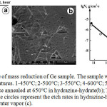 |
Figure 1: Time dependence of mass reduction of Ge sample. The sample was annealed in hydrazine-hydrate at different temperatures. |
1-450°C; 2-500°C; 3-550°C; 4-600°C; 5-650°C (a); Triangular etch pits formed at the Ge surface annealed at 650°C in hydrazine-hydrate(b); The Arrhenius plot of Ge sample etch rates. The white circles represent the etch rates in hydrazine-hydrate, while the black circles show etch rates in water vapor (c).
In the selected temperature range the etch rate varies from 0.5 nm/min up to 235 nm/min. The linear character of graphs in Fig. 1a makes it easy to calculate the etch rates at different temperatures and then to plot the temperature dependence of etch rate (Fig. 1c). The slope of the line in Fig. 1c gives the value of the activation energy for the etching process- EA=201±15 kJ/mol. This value is close to the activation energy of GeO sublimation in vacuum, Ar or N2 (188-221 kJ/mol) obtained by different authors [16,17]. It should be emphasized that the etching of Ge with dry oxygen proceeds also through the formation of volatile GeO suboxides. However, the activation energy for this process is quite different and equals to 377 kJ/mol due to the sublimation of dimeric Ge2O2 molecules [18].
To define the critical role of water molecules in the germanium etching process we have used the pure water vapour. The results are indicated in Fig. 1c by black circles. They show that for the fixed Ge temperatures the etch rates are slightly exceeding those for hydrazine-hydrate, while their energies of activation, calculated from the slope of the curve, coincide (Fig. 1c).
The absence of any synthesized film on the surface of Ge sample indicates that the role of hydrazine decomposition products is negligible and the etching is performed by the following chemical reaction:
Ge(s)+H2O(g)=GeO(g)+H2(g) (1)
It is well known that when reacting with Ge, the water molecules serve as active oxidizers as well as a reducers providing formation of volatile GeO molecules for the mass transfer and growth of different nanostructures like Ge-GeO2 core–shall nanowires and even for the formation of polycrystalline Ge films [19-21]. Annealing of Ge-GeO2 system in conditions similar to our experiments provides a high pressure of GeO vapor (~10-5 Torr) and intensive VLS growth of Ge NWs from the catalyst GeOx ball tips [22].
The results presented in Fig.1 prove that in our experiments the water molecules are actively eroding Ge, forming the intensive flux of volatile monoxide molecules (GeO) which then serve as precursors for the growth of nitride NWs.
The qualitatively different kinetic curves were obtained for the interaction of Ge with hydrazine containing 3mol.% H2O. Fig. 2 presents the data on the mass reduction of Ge sample annealed in hydrazine in the range of 450-520°C.
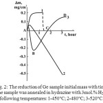 |
Figure 2: The reduction of Ge sample initial mass with time. The sample was annealed in hydrazine with 3mol.% H2O at following temperatures: 1-450°C; 2-480°C; 3-520°C. |
The increase of Ge mass is observed when the Ge sample is annealed at 450°C (Fig. 2, curve 1). This process has a reversible nature, because the initial mass of Ge sample is completely restored after evacuation of a system (the dashed line in Fig. 2, curve 1). The formation of a surface layer was not observed after evacuation, indicating that the mass increase during annealing was caused by the process of a physical adsorption. This type of curves can be ascribed by the kinetic equation of adsorption onto the plane surface [23]:
![]()
were Δm (g/cm2) is the mass increase of a unit area at time t , Δm0 is the maximum value of Dm, k (s-1) is the dsorption rate constant. The temperature dependence of the adsorption rate yields the zero activation energy for this process, indicating that the adsorption has a physical character.
At temperatures close to 500°C the curves have quite different nature. At first the adsorption related portion of a curve gradually decreases with the decrease of Ge mass (Fig. 2, curve 2 and a section AB of the curve 3). This process describes the vapor etching of Ge surface, which is accomplished by the formation and evaporation of volatile germanium containing species. The etch rate can be calculated using the linear portion of the mass reduction curves. The temperature dependence of the etch rate enabled to calculate the activation energy of the etching process. The obtained value (EA=200 kJ/mol), was close to that estimated for GeO evaporation during the annealing of Ge in hydrazine-hydrate. However, the etch rate in hydrazine-hydrate was by two orders of magnitude higher than in hydrazine with 3 mol.% H2O. These results prove that up to 500°C only water molecules interact with Ge sample, while the activity of hydrazine is completely suppressed.
At temperatures exceeding 500°C, after a certain period of time marked by the letter B in Fig. 2, curve 3, the mass of Ge sample gradually increases and a solid product is formed at the surface (Fig. 2, segment BD in the curve 3). As it will be shown later this solid product, which is depicted in Fig. 3a,b, consists of crystalline germanium nitride nanowires. The growth of nitride results in the increase of mass (Fig. 2, segment BCD in curve 3). The segment BC is a straight line, indicating that at first the nitride material is growing at a constant rate. However, the growth rate gradually decreases with time and finally saturates. Diffusion of nitride- forming species through the grown nanowire “mat” is the rate limiting factor of this process, which causes the saturation of the growth rate.
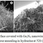 |
Figure 3: Ge surface covered with Ge3N4 nanowire “mat” formed after 1 hour annealing in hydrazine at 520 (a) and 540°C (b). Click here to View figure |
The growth of nanowires needs the permanent supply of Ge and nitrogen precursors. Hydrazine provides nitdriding precursors, while water serves for producing volatile GeO molecules. However, the water content in hydrazine has a critical role in the growth of nanowires, because the excess amount of H2O will cause permanent etching of Ge sample. According to our data, 3-5 mol% of water in hydrazine is the optimal content that ensures the growth of Ge3N4 nanowires.
Fig. 4 represents 1D germanium nitride nanomaterials grown on Ge sample surface at 500 and 520°C. The details of growth technology are described in [24]. The nanowire growth mechanism depended on the Ge temperature. At 500°C they grew through the Vapor-Liquid-Solid (VLS) method with Ge self-catalyst tip (Fig. 4a,b). The growth mechanism was changed to Vapor-Solid (VS) one at 520°C (Fig.4c,d). The mass transfer to the growth front of nanowires was accomplished by volatile GeO molecules sublimated from the Ge source. Because the both, nitride forming and oxidizing precursors were presented in the gaseous phase, we decided to calculate the thermochemical reactions and evaluate the formation of which phase was thermodynamically more favorable. The reactions were calculated for the Ge source temperature of 500°C.
2GeO(g) + O2(g) = 2GeO2 ΔG= -649 kJ/mol (3)
GeO(g)+H2O(g)=GeO2+H2(g) ΔG= -119 kJ/mol (4)
3GeO+4NH3(g)=Ge3N4+3H2O(g) +3H2(g) ΔG= -469 kJ/mol (5)
3GeO+4NH2(g)=Ge3N4+3H2O(g)+H2(g) ΔG= -1196 kJ/mol (6)
3GeO+4NH(g)+H2(g)= Ge3N4 + 3H2O(g) ΔG= -1774 kJ/mol (7)
Comparing the Gibbs free energies for reactions (3)-(6) it becomes clear that the formation of nitrides is thermodynamically more favorable than the synthesis of GeO2. We have not evaluated the kinetic factors for these reactions, but taking into account the high yield of Ge3N4 nanowires one can assume that the kinetic factors of nitride formation are also sufficiently high. It should be noted that the temperature of Ge3N4 nanowire formation in our technology is by 350°C lower than the synthetic temperature of the same nanomaterials in ammonia [25,26]. This proves once again the high activity of hydrazine decomposition products, which, in our opinion, is caused by the increased concentration of NH and NH2 radicals.
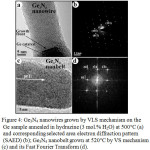 |
Figure 4: Ge3N4 nanowires grown by VLS mechanism on the Ge sample annealed in hydrazine (3 mol.% H2O) at 500°C (a) and corresponding selected area electron diffraction pattern (SAED) (b); Ge3N4 nanobelt grown at 520°C by VS mechanism (c) and its Fast Fourier Transform (d). Click here to View figure |
All synthesized nanowires had the structure of a-Ge3N4. Nor germanium oxide, neither pure germanium nanomaterials were observed. The role of water molecules in the growth of Ge3N4 nanowires is the formation of volatile germanium suboxide molecules on the surface of Ge source, which then serve as precursors for the growth of nanowires through the reactions (4)-(6).
In our previous work, we have produced the pure indium oxide nanowires by annealing the metallic In source in hydrazine+3 mol.% H2O [27]. According to literature [28-30] the only volatile species that can provide the mass transfer of In from source to Si substrate are indium suboxide molecules (In2O). It is well known that water molecules considerably increase the thickness of an oxide layer on the liquid indium droplet [31]. In our experiments the volatile In2O were produced after reduction of oxidized In source surface with hydrogen, NH or NH2 radicals. It was established that when using the metallic indium source, in contrast to Ge source, the nitriding ability of hydrazine decomposition products was completely suppressed, while the oxidizing ability of water diluted in hydrazine was clearly pronounced.
It is worth noting, that after arrival of volatile In2O on the substrate surface, the final product that will be formed from suboxides depends on the environment and a type of co-deposited molecules. In [32,33] it was established, that in the presence of Ga the indium suboxide can be reduce to pure In.
Our next experimental works were aimed at the synthesis of nanowires using the developed hydrazine technology and the InP as a source material, instead of metallic In source. The single crystalline InP source was placed on the bottom of the reactor and annealed in hydrazine. The Si substrate was located at 2 cm above the InP source. The phosphorous vapor was provided after dissociation of InP source at elevated temperatures. It has been reported that the atomic hydrogen, which can be generated via hydrazine decomposition, may reduce the InP decomposition temperature by 230°C, thereby promoting the formation of P2, P3 and PH3 species [34]. Due to the decomposition of InP the phosphorus vapor appeared in the reactor and In droplets were formed on the surface of InP. After that, the indium mass transfer to Si substrate may proceed through the mechanism that was discussed above when considering the growth from the metallic In source.
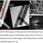 |
Figure 5: HAADF STEM image of InP nanowire with rotational twins (left) and without twins (right), grown in hydrazine with 3 mol.% water (a); corresponding TEM image of nanowires (b); SEM image of InP nanowires (c); SAED pattern of untwined InP nanowire (d). |
Fig.5a shows the High Angle Annular Dark Field (HAADF) scanning TEM image of InP nanowires grown on Si substrate at 440°C after annealing of InP in hydrazine with 3 mol.% H2O. The ordinary TEM and SEM images of nanowires are presented in Fig.5b,c. The twinning is frequently observed in InP nanowires [35,36]. As can be seen in Fig.5a,b, the left vertical nanowire has a structure with random twins, while the right nanowire has no twins. The selected area electron diffraction pattern (Fig.5d) confirmed the formation of InP nanowires with Zinc Blend (ZB) structure. The preferential growth direction is [111] and the calculated value for (111) lattice spacing is 0.340 nm, which agrees well with the d-spacing for this plane in ZB InP. Energy dispersive X-ray (EDX) spectroscopy was applied for the analysis of nanowire composition (Fig. 6a,b). The EDX spectra were taken from rectangular areas depicted in Fig.5a. The oxygen content in nanowires was at the level of background concentration, indicating that the water in hydrazine does not alter the composition of indium phosphide. The XRD pattern (not shown in this paper) also confirmed the formation of InP nanowires with ZB structure.
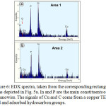 |
Figure 6: EDX spectra, taken from the corresponding rectangular areas depicted in Fig. 5a. In and P are the main constituents of a nanowire. The signals of Cu and C come from a copper TEM grid and adsorbed hydrocarbon groups. Click here to View figure |
The presented results clearly demonstrated that, in spite of similarities of ambient gaseous medium (hydrazine decomposition products with 3 mol.% H2O) and precursors (indium suboxides), the pure In2O3 nanowires were produced in case of In source and the pure InP 1D nanostructures were synthesized when InP source was used. It implies that though the initial ambient was containing the sufficient amount of oxygen to form the indium oxide, in the presence of phosphorous-containing precursors the oxidizing abilities were completely suppressed and the phosphide formation was predominant. This fact does not match the results of calculated thermochemical reactions. These calculations show that the formation of indium oxide is thermodynamically favorable in comparison with the synthesis of phosphide. However, besides thermodynamics, the kinetic factors may play a pivotal role in such a nonequilibrium process as the nanowire growth. Kinetics often may prevail over thermodynamics and the phase, which has a higher growth and nucleation rate, may appear and grow, instead of a more stable and thermodynamically favorable phase [37]. Further investigations are needed to clarify the preferential growth of InP in the presence of water molecules in our technology.
Conclusions
The interaction of crystalline germanium with hydrazine, containing 50 and 3 mol.% H2O was studied in the temperature range of 450-600°C. It was established that up to 500°C only water molecules were reacting with Ge surface causing formation and evaporation of volatile Ge suboxides-GeO. The calculated value of activation energy (201 kJ/mol) was close to the literature data on the sublimation of GeO molecules. At temperatures exceeding 500°C the activity of hydrazine manifests itself and the nitride nanowires start to grow on the Ge surface due to the reactions of GeO with hydrazine decomposition products. Thermochemical reactions confirmed that the formation of germanium nitride is preferable than the synthesis of germanium dioxide.
Preliminary investigation of hydrazine-assisted growth of InP nanowires showed that a small amount of water (3mol.%) diluted in hydrazine served for producing the volatile molecules of indium suboxide – In2O. After reaching the Si substrate these suboxides were reacting with phosphorus vapor forming InP nanowires with zinc blende structure, while the oxidizing ability and the formation of In2O3 nanowires were suppressed in the presence of phosphorous vapor.
Acknowledgements
This work was financially supported by the Shota Rustaveli National Science Foundation Grant PhDF2016_113.
References
- Markoc, H. Nitride semiconductor devices: fundamentals and applications. John Wiley&Sons. 2013.
CrossRef - Fang, M.; Han, N.; Wang, F.; Yang, Z.; Yip, S.; Dong, G.; Hou, J.J.; Chueh, Y.; Ho J. C. J. Nanomater. 2014, 2014, 1-14
CrossRef - Morkotter, S. Structural and electrical characterization of III-V semiconductor nanowires. Verein zur Förderung des Walter Schottky Inst. der Techn. Univ. München, 2015.
- Joice, H.J.; Gao, Q.; Tn, H.H.; Jagadish, C.; Kim, Y.; Zou, J.; Smith, L.M.; Jakson, H.E.; Yarrison-Rice, J.M.; Parkinson, P.; Johnston, M.B. Prog. Quant. Electron. 2011, 35, 23-75.
CrossRef - Mi, Z.; Jagadish, Ch. III-Nitride Semiconductor Optoelectronics, Academic Press. 2017
- Akasaki, I.; Amano, H.; Kito, M.; Hiramatsu, K. J. Cryst. Growth. 1991, 48&49, 666-670.
- Akasaki, I.; Amano, H.; Itoh, K.; Koide, N.; Manabe, K. Inst. Phys. Conf. Ser. 1992, 129, 851-856.
- Davydov, V.Yu.; Klochikhin, A.A.; Seisyan, R.P.; Emtsev, V.V.; Ivanov, S.V.; Bechstedt, F.; Furthmüller, J.; Harima, H.; Mudryi, A.V.; Aderhold, J.; Semchinova, O. Phys. Stat. Sol. (b). 2002, 229, R1-R3.
CrossRef - Kong, X.Y.; Ding, Y.; Yang, R.; Wang, Z.L. Science. 2004, 303, 1348–1351.
CrossRef - Kirkham, M.; Wang, Z.L.; Snyder, R.L. Nanotechnology. 2008, 19, 1-4.
CrossRef - Pan, Z.W.; Dai, Z.R.; Wang, Z.L. Science. 2001, 291, 1947-1949.
CrossRef - Suleiman, K.M. Jumidali, M.M.; Hashim, M.R. J.Appl. Sci.2010, 10, 1001-1005.
- Santos, L.B.; Ribeiro, C. A.; Capela, J. M. V.; Crespi, M. S.; Pimentel, M. A. S.; De Julio, M. J. Therm. Anal. Calorim. 2013,113, 1209-1216.
CrossRef - Pakdehi, S.; Salim, M.; Rasoolzadeh, M. Res. Appl. Mech. Eng. 2014, 3, 21–25.
- Dirtu, D.; Odochian, L.; Pui, A.; Humelnicu I. Centr. Eur.J. Chem. 2006, 4, 666–673.
- Arslambekov, V.A. On the mechanisms of formation and sublimation of oxide films on silicon and germanium. Nauka. 1964.
- Inoue, M.; Jap. J. Appl. Phys. 1972, 11, 1147-1152.
CrossRef - Rojansky, N.V. Thesis. Moscow. 1985.
- Hsu, T.J.; Ko, Ch.Y.; Lin, W.T. Nanotechnology. 2007,18, 1-4.
- Lo, W.L.; Chang, H.C.; Hsu, T.J.; Lin, W.T. Jpn. J. Appl. Phys. 2008, 47, 3299-3302.
CrossRef - Lever, R.F.; Jona, F. J. Appl. Phys. 1963, 34, 3139-3140.
CrossRef - Sutter, E.; Ozturk, B.; Sutter P. Nanotechnology. 2008, 19, 435607-5.
CrossRef - Timofeev, D.P. Adsorption Kinetics. Moscow, Academy of Sciences Publishing. 1962.
- Jishiashvili, D.; Kiria, J.; Shiolashvili, Z.; Makhatadze, N.; Miminoshvili, E.; Jishiashvili A. J. Nanosc. 2013, 2013, 1-10.
- Gao, Y. H.; Bando, Y.; Sato, T. Appl. Phys. Lett. 2001, 79, 4565–4567.
CrossRef - Xie, T.; Jiang, Z.; Wu, G.; Fang, X.; Li, G.; Zhang, L. J. Cryst. Growth. 2005, 283, 286–290.
CrossRef - Jishiashvili, D.; Kiria, L.; Shiolashvili, Z.; Makhatadze, N.; Miminoshvili, E.; Jishiashvili, A.; Sukhanov, D. Nano Studies. 2012, 6, 115-120.
- Kam, A.; Kumar, M.; Sinjih, V.N.; Mehta, B. R.; Aravindan, S.; Singh, J. P. Chem.Vap. Deposition, 2012, 18, 295-301.
CrossRef - Yan, Y.; Y. Zhang, Y.; Zeng, H.; Zhang, J.; Cao, X.; Zhang, L. Nanotechnology. 2007, 18, 1-6.
- Ismardi, A.; Dee, C.F.; Hamzah, A.A.; Bais, B.; M.M. Salleh, M.M.; Majlis, B.Y.; Gebushuber, I.C. Sains Malays. 2012, 41, 459-463.
- Schoeller, H.; Choa, J. J. Mater. Res. 2009, 24, 386-393
CrossRef - Vogt, P.; Bierwagen, O. Appl. Phys.Lett. 2016, 109,1-4.
CrossRef - Vogt, P.; Bierwagen, O. AIP APL Materials. 2016, 4, 1-6.
- Gorbenko, V. I.; Gorban A. N. Radiophysics. 2012, 1, 7-10.
- Algra, R.E.; Verheijen, M.A.; Borgström, M.T.; Feiner, L.-F.; Immink, G.; van Enckevort, W.J.P.; Vlieg, E.; Bakkers, E.P.A.M. Nature. 2008, 456, 369–372.
CrossRef - Xiong, Q.; Wang, J.; Eklund, P.C. Nano Lett. 2006, 6, 2736–2742.
CrossRef - Mullin, J.W. Crystallization, Reed Educational and Professional Publishing Ltd, 2001.

This work is licensed under a Creative Commons Attribution 4.0 International License.
![]()
A New Edition of Web of Science
Journal Impact Factor
2022: 0.5
Five Year: 0.8
Journal is Indexed in

Cabells Whitelist
![]()


