Photochemical Method of Applying Gold films on the Dielectric Surfaces
Sataev M.S, Abdurazova P. A, Koshkarbaeva Sh.T., Tleuova A.B and Aueshov A.P.
Koshkarbaeva, Aiym Bolatbekovna Tleuova, Auyeshov Abdrazakh Pernebaevich South Kazakhstan State University named after M. O. Auezov, Shymkent, Kazakhstan.
Corresponding Author E-mail: malik_1943@mail.ru
DOI : http://dx.doi.org/10.13005/ojc/330232
Article Received on : December 01, 2016
Article Accepted on : March 17, 2017
A method of photochemical application of gold films on the dielectric surfaces is offered. At this initially by dipping of sample in a solution of gold chloride the sorption layer of the solution is created on the surface. Then, the drying process is carried out under direct sunlight. As the drying of the sorption layer the conditions are created for the formation of monovalent gold chloride having semiconducting properties that allows gold reducing photochemical reaction to take place. Carrying out the process at room temperature in the absence of a reducing agent simplifies a gilding technology. A study of photochemical gilding textile using the scanning electron microscope ISM-6490-LV (JEOL, Japan) is showed that the degree of transition of gold on the surface of a textile is greater than 97%.
KEYWORDS:Gold; reduction mechanism; gold film; semiconducting properties; photochemical method
Download this article as:| Copy the following to cite this article: Sataev M.S, Abdurazova P. A, Koshkarbaeva Sh.T., Tleuova A.B, Aueshov A.P.. Photochemical Method of Applying Gold films on the Dielectric Surfaces. Orient J Chem 2017;33(2). |
| Copy the following to cite this URL: Sataev M.S, Abdurazova P. A, Koshkarbaeva Sh.T., Tleuova A.B, Aueshov A.P.. Photochemical Method of Applying Gold films on the Dielectric Surfaces. Orient J Chem 2017;33(2). Available from: http://www.orientjchem.org/?p=31256 |
Introduction
Due to several features of the physical-chemical properties a gold coating of dielectrics is widely used in engineering. These features include: corrosion resistance, high electrical and thermal conductivity, low and stable contact resistance over time, catalytic and bactericidal activity, as well as decorative look.
In accordance with the fields of application of coatings the various methods of applying gold on the dielectric surfaces are developed [1-3].
There is widespread chemical gilding with the use of cyanide, ferrocyanide, chloroauric electrolytes, containing dimetilboran, hydrazine sulphate, sodium hypophosphite, citrate or tartaric acid salts as a reducing agent [4-6]. The main disadvantage of chemical methods is that when gilding dielectrics must be pre-coated on their surfaces by copper, nickel, silver. Wherein mentioned surfaces can be coated by gold without the use of a reducing agent using the method of immersion (contact) gilding [7-11] that occurs by substitution reaction of underlying metal to gold. Increasing the thickness of the coating takes place until all the surfaces coated by gold, therefore the method has limitations on coating thickness (no more than 0.2 µm).
Chemical deposition of gold on the porous metal oxide dielectrics can be carried out without previous metallization. For this purpose, they were firstly treated by an aqueous solution of aurichlorohydric acid (AuCl3 dissolved in hydrochloric acid), dried at temperatures from 60 °C to 200 °C, and then reduced at temperatures above 250°C in hydrogen flow using chemical reductants for 80 – 120 minutes [12].
As well the physical methods are used for gilding dielectrics. There is the method of deposition of gold nanoparticles on silica microspheres, based on thermal decomposition of volatile compounds of gold. Thus, use of vapors of a volatile organometallic complex of dimethylgold dipivaloylmethanates, which at appropriate temperatures in vacuum is reduced forming the microspheres on the surface of gold nanoparticles [13].
To form a coating made of noble metals and their alloys, a method is proposed [14] of magnetron spreading of target cathode of precious metals or their alloys by ions with energy, enough to move metal atoms or their groups to the substrate.
Photochemical synthesis of nanoparticles of copper, silver and gold on polymer microspheres surfaces implemented in the works [15-17]. It is noted that in this case polymer microsphere surfaces, performing sorption centres function of metal nanoparticles, allow to form stable dispersions. A disadvantage of this method is that photochemical reaction with the formation of gold occurs only at certain dielectric structure and it allows obtaining only the nano-sized films, which significantly narrows the field of application of the method. The basis of the proposed work is a photochemical method of gold recovery by the action of solar beams.
Materials and Methods
The scheme of photochemical dielectrics gilding is shown in Figure 1. At this initially a dielectric is processed by known in electroplating methods to impart its surface wettability. In case of cotton textile this procedure is unnecessary. Then sample is immersed for 1-3 minutes in 1-20 g/l auric chloride solution. Wherein on the sample surface a sorption layer of auric chloride remains (Fig. 1, a).
Influence of solar beams (Fig. 1, b) leads to a double effect on the dielectric surface: the first is to accelerate the drying process of the sorption layer and secondly leads to photochemical reactions. The first process leads to a thickening of the auric chloride solution, which makes it possible to form AuCl, which crystallization starts on a solid phase surface of the dielectric, what is the source crystallization centers (Fig. 1, c).
On the resulting crystals of AuCl semiconductor under influence of solar beams take place the formation of gold metal and the oxygen release (Fig. 1, d).
As the drying a semiconductor region is shifted outside of the adsorption layer (Fig. 1, e) and there is a gradual filling of layer with gold. The metallic gold formation process can be determined by electron and “holes” migration in the semiconductor. As a result of photochemical reactions a dielectric is covered with a dark color film, typical to gold, obtained from salt solutions using various reducing agents.
When film is fully dried the outer surface of the film is coated with auric chloride what was not participated at the reduction reaction and is coated with by-product НCl (Fig. 1, f). This is water-soluble products and is easily washed out with water (Fig. 1, g). In this way, after these operations metallic gold film on a dielectric surface is obtained.
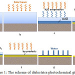 |
Figure 1: The scheme of dielectrics photochemical gilding Click here to View Figure |
The elementary composition of the film in various samples was studied using the scanning electron microscope ISM-6490-LV (JEOL, Japan).
Results and discussion
A sample of cotton textile for 3 minutes was dipped in a solution containing 10 g/l AuCl3. Then by shaking the excess solution of gold chlorine was removed. Then the sample was illuminated by sunlight. Some areas were screened by the opaque disk made of polymeric material (Fig. 2).
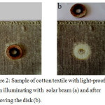 |
Figure 2: Sample of cotton textile with light-proof disk when illuminating with solar beam (a) and after removing the disk (b). Click here to View Figure |
When sample is fully dried a black film was formed only on the lighted areas (Fig. 2).
The sample was washed with distilled water from not involved into a photochemical reaction auric chloride and reaction by-products and then dried in air.
Electron picture and elementary composition of origin textile is shown in Figure 3.
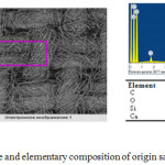 |
Figure 3: Electron picture and elementary composition of origin sample of the cotton textile Click here to View Figure |
Figure 4 shows border sections of textile, illuminated by solar beam and darken with opaque disk. In this darkened areas a dark color have retained which is peculiar to origin textile, and illuminated sections acquired bright colors peculiar to metals.
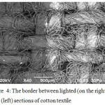 |
Figure 4: The border between lighted (on the right) and dark (left) sections of cotton textile Click here to View Figure |
In the dark by opaque disk sections of textile (Fig. 5) textile color is not changed, only in certain areas observed small bright points. Elemental analysis shows, that except elements characteristic of the original textile (carbon, oxygen, silicon, calcium) added little gold and chlorine. This indicates that the bulk of the water-soluble auric chloride layer in these areas, in a result of the operation remains unchanged, and is removed by washing with water.
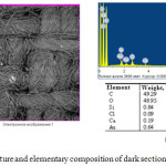 |
Figure 5: Electron picture and elementary composition of dark sections of sample surface. Click here to View Figure |
On the illuminated sections in the result of conducting photochemical reactions the layer of elementary gold if formed (Figure 6). At this, if to take into account that surface layer contains 0,02 atomic % of chloride, which bonds the same amount of atomic % of gold into insoluble AuCl, and the general composition is 0,60 atomic %, then more than 97% of gold on the surface is in the state of metal.
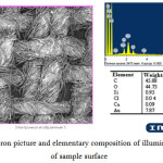 |
Figure 6: Electron picture and elementary composition of illuminated sections of sample surface Click here to View figure |
The rest of the amount of gold, less than 3%, probably in the form of chloride, which is not yet in a photochemical reaction, for various reasons. This may be due to the fact some particles of auric chloride AuCl, located in the pores of the dielectric, lost contact with the main part of the semiconductor and because of the shielding previously allocated of gold particles not subjected to a photochemical reaction.
A film thickness depends on the auric chloride concentration in sorption layer. Thus at a concentration of 1 g/l to 20 g/l the film thickness ranges from 10 nm to 0,2 µm.
A photochemical reaction occurs in the sorption layer of gold chloride solution on the dielectric surface. In this system, a possible reaction is the formation of monovalent gold ions.
2Au3+ + 2 H2O =2 Au+ + O2 + 4 H+ (1)
Thermodynamically this reaction is possible, as the standard reaction potential
Au3+ +2e = Au+ Eo = 1.401 B, (2)
is positive than the standard reaction potential
O2 + 4 H+ +4e = 2 H2O Eo = 1.229 B. (3)
Under normal conditions, the direction of reaction (1) strongly shifted to the left, therefore selection appreciable amounts AuCl, as well as oxygen and HCl not observed.
As the drying of the sorption layer is an increase AuCl3 concentration, which increases the oxidative capacity of trivalent gold. This increases the possibility of the reaction proceeds, which leads to the formation of sparingly soluble in this medium of monovalent gold.
In addition, the sorption contacting layer to a solid surface, constituting the crystallization centers, facilitates the appearance of solid-layer AuCl.
Chloride monovalent gold has semiconducting properties and therefore when exposed to light it becomes possible to flow a photochemical reaction.
![]()
The progress of the photoreaction shifts the 1 reaction equilibrium to the right, and the overall reaction in this case takes the form:
2AuCl3 + 3H2O→ 2Au + 3/2О2 + 6НCl (5)
Conclusions
Thus, to obtain gold films it is enough to create on the surface of the dielectric a sorption layer of AuCl3 solution and subjected to drying under the influence of solar beam. Wherein the gradual drying of sorption layer leads to appearance of semiconductor particles of AuCl, which under an influence of solar beam by photochemical reaction form on the surface more than 97% of gold as a metal, what simplifies the technology of dielectrics gilding.
References
- Arora A. K, Jaswal V. S, Singh K, Singh R. Applications of Metal/Mixed Metal Oxides as Photocatalyst: A Review. Orient J Chem .,2016.,32(4). 2035-2042.
- Khorshidi N, Khorrami S. A, Olya M. E, Mottiee F. Photodegradation of basic dyes using nanocomposite (Ag-zinc oxide-copper oxide) and kinetic studies. Orient J Chem .,2016;32(2) 1205-1214.
- Koshkarbaeva T.Sh., Nauryzova S. Z, Sataev M. S, Tleuova A. B. Low-Temperature Gas-Phase Metallization of Dielectrics. Orient J Chem .,2012.,28(3) 1281-1283.
- Himicheskoe osajdenie metallov iz vodnyh rastvorov. / Edited by V. V. Sviridova. Minsk: Universitetskoe. 1987, 270.
- Mel’nikov, P.S. Spravochnik po gal’vanopokrytiyam v mawinostroenii, 1979. Patent US 4999054, 1991.
- IPC-4552. Specification for Electroless Nikel / Immersion Gold (ENIG) Plating for Printed Circuit Boards, July 2002.
- Shkundina S. Novye processy i materialy v proizvodstve pechatnyh plat // Tehnologii v elektronnoi promyshlennosti, 2009, 4.
- Osaka T., Misato T., Sato J., Akiya H., Homma T., Kato M., Okinaka Y. and Yoshioka O. Evaluation of Substrate (Ni)‐Catalyzed Electroless Gold Plating Process. J. Electrochem. Soc. 2000; 147(3), 1059-1064.
- Medvedev A., Nabatov Yu., Semenov P., Shkundina S. Immersionnoe zolochenie pod paiku. J. Tehnologiya v elektronnoi promyshlennosti 2010. 2
- Patent BU 10283, IPC C23С18/31, pub. 2008.02.18. Rastvor dlya bezelektroliznogo osajdeniya plenok zolota na nikelevye pokrytiya.
- Hadji Begli A., Baats K., Dekker N., Pryusse U., Forlop K-D. Zolotoi katalizator na nositele RU 2378048, bulletin published. №1 from 10.01.2010.
- Patent RF № 2489230 IPC: B22F9/12. Sposob osajdeniya nanochastic zolota na mikrosfery kremnezyoma, osnovannyi na termicheskom razlojenii letuchih soedinenii zolota / Kuch’yanov A.S., Plehanov A.I., Igumenov I.K., Kuchumov B.M., Parhomenko R.G., Trubin S.V. Published 10.08.2013.
- Patent RF № 2214476 MPK: C23C14/16. Sposob formirovaniya pokrytiya iz dragocennyh metallov i ih splavov / Tuleuwev A.J., Lisicyn V.N., Tuleuwev Yu.J., Volodin V.N., Kim S.N. Published 20.10.2003.
- Isaeva E. I., Svistunova O. B., Gorbunova V. V., Boicova T. B. Fotohimicheskii sintez nanochastic zolota v elastomernyh plenkah polibutilakrilatnogo lateksa. J. general chemistry, 2007; 77(12), 1968-1971.
- Isaeva E. I., Boicova T. B., Gorbunova V. V. Fotohimiсрeskii sintez nanoсрastic zolota v lateksah. J. applied chemistry. 2006; 79(4), 683-685.
- Sacher Е., Pireax J. J., Kowalczyk S.P. (Eds.) Metallization of Polymer. // Washington D.C.: ACS, Symp.Ser. 1990; 440(1), 282-288.

This work is licensed under a Creative Commons Attribution 4.0 International License.
![]()
A New Edition of Web of Science
Journal Impact Factor
2022: 0.5
Five Year: 0.8
Journal is Indexed in

Cabells Whitelist
![]()


