Application of the Spark Discharge Generator for Solvent-free Aerosol Jet Printing
Alexey Efimov1, Gleb Potapov2, Anton Nisan2, Maxim Urazov1 and Victor Ivanov1
1Moscow Institute of Physics and Technology, Dolgoprudny, Russia.
2Ostec Enterprise Ltd., Moscow, Russia.
Corresponding Author E-mail: efimov.aa@mipt.ru
DOI : http://dx.doi.org/10.13005/ojc/330264
A new solvent-free method of aerosol printing for fabrication conductive structures in the form of lines with a minimum width of 60 µm and an average thickness of up to 6 µm has been proposed and investigated. This method is based on dry deposition of focused beam of silver nanoparticles synthesized by the multi-spark discharge generator. Printed and sintered microstructures showed low electrical resistivity equal to 7.5 μΩ∙cm, which is five times greater than the resistivity of bulk silver. The described method of dry aerosol printing without solvents could be a promising alternative to conventional «wet» aerosol jet printing.
KEYWORDS:Aerosol jet printing; Spark discharge generator; Aerodynamic focusing; Nanoparticles
Download this article as:| Copy the following to cite this article: Efimov A, Potapov G, Nisan A, Urazov M, Ivanov V. Application of the Spark Discharge Generator for Solvent-free Aerosol Jet Printing. Orient J Chem 2017;33(2). |
| Copy the following to cite this URL: Efimov A, Potapov G, Nisan A, Urazov M, Ivanov V. Application of the Spark Discharge Generator for Solvent-free Aerosol Jet Printing. Orient J Chem 2017;33(2). Available from: http://www.orientjchem.org/?p=31032 |
Introduction
Aerosol jet printing is a promising method for fabrication of printed electronics goods, such as sensors1,2, solid oxide-fuel cells3, solar cells4 and organic LEDs5. The conventional approach of aerosol jet printing is based on the selective deposition of focused beams of microdroplets on a substrate with nanoparticles inside6. Microdroplets are obtained from nano-inks based on organic solvents, which are sprayed by a pneumatic or ultrasonic generator7. The use of nano-ink causes some significant problems: 1) environmental pollution due to the use of organic solvents; 2) requirements to the conditions and terms for storage of the inks; 3) necessity of removing and recycling solvent and surfactant after deposition8. In this regard, researchers are developing and investigating the new environmentally friendly and versatile source of nanoparticles for aerosol jet printing, which does not require the use of inks with solvents.
It is known that the pulsed discharge allows to obtain chemically pure nanoparticles of various metal9,10 and semiconductor11 materials in the processes of electric erosion of electrodes at controlled energy efficiency12,13 and high environmental friendliness10 of the synthesis process. Moreover, due to the agglomeration of nanoparticles into large particles with a size of 20-300 nm, the particles can be aerodynamically focused. The deposited material has high activity for sintering at low temperatures14 because the agglomerates are composed of primary nanoparticles smaller than 10 nm. It is important to perform the aerosol printing on plastic substrates15. In this research, we investigated the possibility of using the multi-spark discharge generator for the realization of solvent-free process of aerosol printing of microstructures.
Experimental
The experimental setup consisted of a multi-spark discharge generator16,17 and a commercial system for the particle deposition AJ 15XE (Neotech AMT GmbH) with coaxial nozzle 100 μm in outlet diameter (Fig. 1). Aerosol nanoparticles 1 were synthesized by the multi-spark discharge generator 2 as a result of electrical erosion of silver electrodes 3 in air. Aerosol nanoparticles were directed into the deposition system using a pump 4. The deposition system 5 consisted of a coaxial nozzle 6 with a regulator of sheath gas and the coordinate table 7 to move the substrate 8. In the gas flow nanoparticles united into agglomerates9,17, the size of which depends on the particle concentration and the residence time of aerosol. Inlet pressure in the deposition system was kept constant by a reducer 9. The aerosol flow Qa entered the coaxial nozzle through the inner cylindrical channel, while the sheath flow Qsh was inserted through the outer conically converging axisymmetrical channel. Thus the particle movement from the central line of the flow was prevented, while the hydrodynamic focusing of the aerosol beam was provided. Then the focused aerosol beam 10 was directed to the glass substrate for deposition. The effective deposition of nanoparticles on the substrate occurred when the distance between nozzle and substrate was about 0.5 mm. In the process of moving the substrate relatively to the focused aerosol beam at speed of motion about 10 mm/min, we formed the line of deposited silver nanoparticles on the substrate. The width of the deposited line is controlled by changing the sheath flow rate Qsh from 35 to 100 sccm at a fixed flow rate of the aerosol Qa. The formation of a line of sufficient thickness is ensured by multiple passes of printing. Printed lines were annealed in a muffle furnace at 450°C for 1 hour in the air atmosphere.
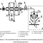 |
Figure 1: The experimental setup for solvent-free aerosol printing using the multi-spark discharge generator. Click here to View figure |
Aerosol nanoparticles were characterized by the aerosol spectrometer SMPS 3936, before their entering the nozzle. Additionally, we investigated the size and morphology of nanoparticles entering the nozzle by the transmission electron microscope (TEM) JEM-2100. The width of formed lines was measured by the optical microscope KH-7700. The microstructure, cross-sectional profile and thickness of the line was studied using scanning electron microscope (SEM) JSM-7001F. The cross-sectional profile and thickness was also measured using the profilometer DektakXT, while the electrical resistivity of the printed and sintered lines by using the four-probe method.
Results and Discussion
Figure 2 demonstrates the particle size distribution at the stage of entering the nozzle from electrical mobility measurements in the aerosol and TEM-image of such nanoparticles (see the insertion). It has been found that while entering the nozzle the size of agglomerates is in the range from 15 to 100 nm, and their mean size is about 44 nm. In this case, the agglomeration of particles is a positive process because it allows the aerodynamic focusing and inertial deposition of agglomerated nanoparticles. Figure 3 shows the images of lines which prove the ability of focusing and inertial deposition of silver nanoparticles synthesized by the multi-spark discharge generator. This figure demonstrates the influence of sheath flow rate Qsh on the width of the deposited lines measured in the optical microscope. Figure 3 demonstrates that the increasing of the sheath flow rate Qsh from 35 to 100 sccm leads to the decreasing the width of lines by more than 2 times, from 163 to 86 μm, respectively. The dependence of the line width from the sheath flow rate Qsh isdue to the fact that the diameter of the aerosol beam Db also depends on the sheath flow18:
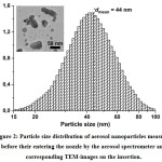 |
Figure 2: Particle size distribution of aerosol nanoparticles measured before their entering the nozzle by the aerosol spectrometer and corresponding TEM-images on the insertion.
|
where Dn is nozzle outlet diameter.
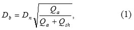
Equation (1) shows that an increase of the sheath flow rate Qsh at a constant flow rate of aerosol Qa leads to a decrease in the diameter of the aerosol beam Db and as a consequence a decrease of the line width (Fig. 3).
 |
Figure 3: Images of lines of deposited nanoparticles related to the sheath flow rate Qsh. Click here to View figure |
Figure 4a shows a typical SEM image of the cross-section of the line corresponding to the image in Fig. 3d. The cross-section profile of the printed line has a bell-shaped form with maximum thickness and width equal to 12 and 56 µm, respectively. In the array of sintered particles small pores with a total area of about 20 µm2 were found. Figure 4b also shows the section profile of the line, measured by the profilometer. The cross-sectional area and average thickness of the line was 350 µm2 and 6 µm, respectively. The average thickness of the line was determined by dividing the cross-sectional area by the line width. It has been proved that the shapes of the profiles measured by the scanning electron microscope and profilometer correlated well.
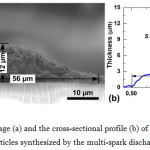 |
Figure 4: The SEM image (a) and the cross-sectional profile (b) of a sintered line formed of deposited silver nanoparticles synthesized by the multi-spark discharge generator. Click here to View figure |
Using the results of measurements of cross-sectional area, the length and line resistance, the electrical resistivity of the formed lines, which amounted to about 7.5 μΩ∙cm. was determined. This resistivity value is approximately 5 times higher than the electrical resistivity of bulk silver, but it is sufficient for some practical applications, e.g. for the production of microheaters, interconnectors, microstrip antennas, gas flow sensors etc.
Conclusions
We proposed and investigated the solvent-free method of direct aerosol printing of microstructures by dry deposition of the focused beam of silver nanoparticles synthesized by the multi-spark discharge generator. Printed microstructures had a width, average thickness and resistivity equal to 60 µm, 6 µm and 7.5 μΩ∙cm, respectively. The same microstructures can be used in printed electronics devices. The proposed solvent-free method is a promising alternative to the conventional method of «wet» aerosol jet printing.
Acknowledgements
This work was supported by the Russian Science Foundation (project # 15-19-00190).
References
- Vasiliev, A. A.; Sokolov, A. V.; Legin, A. V.; Samotaev, N. N.; Oblov, K. Y.; Kim, V. P.; Tkachev, S. V.; Gubin, S. P.; Potapov, G. N.; Kokhtina, Y. V.; Nisan, A. V. Procedia Eng. 2015, 120, 1087–1090.
CrossRef - Liu, R.; Ding, H.; Lin, J.; Shen, F.; Cui, Z.; Zhang, T. Nanotechnology 2012, 23, 505301.
CrossRef - Sukeshini A., M.; Meisenkothen, F.; Gardner, P.; Reitz, T. L. J. Power Sources 2013, 224, 295–303.
CrossRef - Yang, C.; Zhou, E.; Miyanishi, S.; Hashimoto, K.; Tajima, K. ACS Appl. Mater. Interfaces 2011, 3, 4053–4058.
CrossRef - Tait, J. G.; Witkowska, E.; Hirade, M.; Ke, T.-H.; Malinowski, P. E.; Steudel, S.; Adachi, C.; Heremans, P. Org. Electron. 2015, 22, 40–43.
CrossRef - Seifert, T.; Sowade, E.; Roscher, F.; Wiemer, M.; Gessner, T.; Baumann, R. R. Ind. Eng. Chem. Res. 2015, 54, 769–779.
CrossRef - Navratil, J.; Hamacek, A.; Reboun, J.; Soukup, R. In 2015 38th International Spring Seminar on Electronics Technology (ISSE); 2015; pp. 36–39.
- Dearden, A. L.; Smith, P. J.; Shin, D.-Y.; Reis, N.; Derby, B.; O’Brien, P. Macromol. Rapid Commun. 2005, 26, 315–318.
CrossRef - Efimov, A.; Lizunova, A.; Sukharev, V.; Ivanov, V. Korean J. Mater. Res. 2016, 26, 123–129.
CrossRef - Ludvigsson, L.; Meuller, B. O.; Messing, M. E. J. Phys. Appl. Phys. 2015, 48, 314012.
CrossRef - Vons, V. A.; Smet, L. C. P. M. de; Munao, D.; Evirgen, A.; Kelder, E. M.; Schmidt-Ott, A. J. Nanoparticle Res. 2011, 13, 4867–4879.
CrossRef - Mylnikov, D. A.; Efimov, A. A.; Ivanov, V. V. J. Nano- Electron. Phys. 2016, 8, 3052-1-3052–3.
- Myl’nikov, D. A.; Ivanov, V. V.; Efimov, A. A.; Beketov, I. V. Meas. Tech. 2016, 58, 1367–1371.
CrossRef - Peng, P.; Hu, A.; Gerlich, A. P.; Zou, G.; Liu, L.; Zhou, Y. N. ACS Appl. Mater. Interfaces 2015, 7, 12597–12618.
CrossRef - Ko, S. H.; Pan, H.; Grigoropoulos, C. P.; Luscombe, C. K.; Fréchet, J. M. J.; Poulikakos, D. Nanotechnology 2007, 18, 345202.
CrossRef - Efimov, A. A.; Ivanov, V. V.; Bagazeev, A. V.; Beketov, I. V.; Volkov, I. A.; Shcherbinin, S. V. Tech. Phys. Lett. 2013, 39, 1053–1056.
CrossRef - Efimov, A.; Sukharev, V.; Ivanov, V.; Lizunova, A. Orient. J. Chem. 2015, 31.
- Park, J.; Jeong, J.; Kim, C.; Hwang, J. Aerosol Sci. Technol. 2013, 47, 512–519.
CrossRef

This work is licensed under a Creative Commons Attribution 4.0 International License.
About The Author
![]()
A New Edition of Web of Science
Journal Impact Factor
2022: 0.5
Five Year: 0.8
Journal is Indexed in

Cabells Whitelist
![]()


