Photoelectrochemical splitting of water to produce a power appetizer Hydrogen: A green system for future –( A short review)
Pushpendra Kumar*
Department of Chemistry, Lovely Professional University, Phagwara, Punjab – 14411
Corresponding Author E-mail: pushpendra.kmr1@gmail.com
DOI : http://dx.doi.org/10.13005/ojc/320321
Article Received on : May 17, 2016
Article Accepted on : June 27, 2016
Article Published : 09 Jun 2016
To meet the future energy demand, Hydrogen has been accepted as a fuel for future. Out of several renewable methods to produce hydrogen, solar assisted splitting of water (Photoelectrochemical splitting of water) is emerging as a most desired method to produce hydrogen which is a advancement of Photovoltaic process. However, the efficiency of PEC cell is a matter of concern. Various strategies have been adopted by different researchers to increase the efficiency of the system especially using nanotechnology as a tool. In this article, attempts have been made to summarise different approaches applied to obtain effective and viable photoelectrochemical system for splitting water to obtain hydrogen an energy carrier.
KEYWORDS:Splitting of water; Hydrogen; Photoelectrochemical cell
Download this article as:| Copy the following to cite this article: Kumar P . Photoelectrochemical Splitting of Water to Produce A Power Appetizer Hydrogen: A Green System for Future –( A Short Review). Orient J Chem 2016;32(3). |
| Copy the following to cite this URL: Kumar P . Photoelectrochemical Splitting of Water to Produce A Power Appetizer Hydrogen: A Green System for Future –( A Short Review). Orient J Chem 2016;32(3). Available from: http://www.orientjchem.org/?p=17329 |
Introduction
Energy is the most important strategic issue shaping the economy of any nation especially for the developing countries1. The rate of consumption of fossil fuels is increasing exponentially while that of formation is very low. Therefore, we are at the dusk of conventional energy resources. Moreover, we have uneven distribution of energy reserves throughout the world. In the quest of energy crisis we need a new energy system which can replace current energy system so that proper civilisation of energy can be made i.e. energy should be available at each and every point of consumer at reasonable rate. In this respect, hydrogen is emerging as a favourite alternative energy source due to its valuable properties3. It has high energy to weight ratio (144 MJ/kg)4 in comparison to methanol (20 MJ/kg), diesel (46 MJ/kg) and gasoline (44 MJ/kg), High Heat of combustion 34.18 kcal/g compared to petroleum (~10.32 kcal/g), High Energy storage capacity/mole 119 kJ/g (H2) compared to oil (40 kJ/g ). Combining all of these properties, Hydrogen has potential to replace fossil fuels especially for transportation of vehicles. Another most important point is that the end product after combustion of hydrogen is only water which is absolutely safe for the environment and can be recycled. The hydrogen can be used directly as a fuel in vehicles and electricity can be generated by hydrogen using fuel cell5,6. So hydrogen has all properties to replace the conventional energy system. The schematic diagram of hydrogen energy system is depicted in Fig 1. The implementation of hydrogen energy system basically involves production, Storage, Distribution and application as a fuel in engine and fuel cell. Here, production and storage of hydrogen is the area of concern. We have many methods for hydrogen production but the crucks of the problem is that it should not cause any irreversible damage to the environment. To meet tomorrow’s demand of cheap, environment friendly, renewable and efficient ways of its production are needed like solar assisted splitting of water into hydrogen7, hydrogen production by solid waste8, biological hydrogen production9.
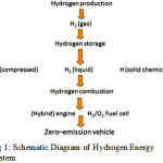 |
Figure 1: Schematic Diagram of Hydrogen Energy System Click here to View figure |
Solar Assisted Splitting of Water
A process that holds a high promise, is extracting hydrogen by direct splitting of water using solar energy using Photoelectrochemical (PEC) way. In this method, light striking the surface of semiconductor material generates electricity and is utilized for electrolysis of water to produce hydrogen and oxygen10. So this method provides a direct pathway to produce hydrogen by using sunlight and eliminates the need to generate the electricity from solar energy and subsequently feeding into an electrolyser as is in the case of photovoltaic-electrolysis system. The schematic diagram of Photoelectrochemical cell is shown in Fig 2. The first demonstration of PEC cell was made Fushishima and Honda11.
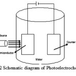 |
Figure 2: Schematic diagram of Photoelectrochemical cell |
The working of PEC cell involves following basic steps a) Production of electron – hole pairs on illumination of semiconductor surface b) Migration of charge carriers: Electrons migrate towards counter electrode by external circuit and holes migrate towards semiconductor – electrolyte interface. c) Holes (h+) oxidizes water to H+ and at counter electrode H+ is reduced to H2. At anode: 2h+ + H2O → ½ O2 + 2H+ At cathode: 2H++ 2e– → H2When light (where hu ³ band gap (Eg) of semiconductor) strikes the surface of semiconductor, electron – hole pairs are generated and due to the presence of electric field, the electron hole pairs existing in the depletion layer get separated and participate in redox processes at the semiconductor – electrolyte interface resulting in the evolution of H2 and O2 at cathode and anode, respectively, by splitting of water. The complete cycle of flow of electrons and the resulting redox processes occurring in a typical PEC cell has been depicted in Fig 3. The splitting of water into H2 and O2 is an endothermic reaction and requires energy of 1.23 eV. Thus, band gap of semiconductor necessary for photoelectrolysis of water should be 1.23 eV. But, factors like overpotential, resistance, loss of electrons etc. makes the semiconductor with a larger band gap (1.8 to 2.2 eV) more suitable12. However, semiconductors with band gap more than 2.4 eV are not desirable because they will not be able to absorb much of the radiations falling in the visible portion of the solar spectrum. It is important to note that much of the energy falling from the sun on earth lies in the visible region. Apart from the selection of a suitable semiconductor of desired band gap, its energetic (band edge energies) should match with energetic of H2 and O2 evolution reaction13.
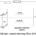 |
Figure 3: Galvanic contact showing flow of electrons |
Therefore, principally, The heart of PEC cell (Figure 2), producing hydrogen, is the semiconductor electrode, which is responsible for absorption of solar radiations and should have strong optical absorption, high electron mobility, long life time of charge carriers, band edges straddling water redox potentials, stable in aqueous environment and low cost. However, till date no semiconductor is available which fulfills all favorable properties.
Semiconductor Photoelectrodes
Metal oxide semiconductors, organic and polymer-based composites are possible candidates for photoelectrodes. Among these, inorganic semiconductor oxides such as TiO214, ZnO15, Fe2O316, CuO17, CdS18, CdSe19 etc. have attracted considerable interest since they satisfy several of the aforementioned requirements. However, no semiconductor fulfils all the requirement pertaining to Photoelectrochemical splitting of water. For efficient PEC system, the semiconductor material must have strong absorption power in visible region for desired photon to hydrogen conversion efficiency. Cu2O, Fe2O3, CdS absorb in visible region but are not stable in aqueous medium. The band edges of Fe2O3 and Cu2O are not in agreement for PEC spitting of water and electron mobility of these material is also poor so they do not offer effective charge separation. On the other hand wide band gap metrial like ZnO or TiO2 satisfy all the requirements for efficient photoelectrochemical system but only the drawback associated with them is that they absorb in UV region. ZnO has high electron mobility20 (100 times more than TiO2). Ternary oxides like CuWO421, BiVO422, ZnWO423 have also emerged as a potential material for PEC splitting of water. These oxides have metal d orbital and oxygen 2 p orbital contributing to the valance band maxima. Olivier et al22 recorded a significant photocurrent with BiVO4 and hydrogen production rate was 0.15 mmol/h under electric bias of 1.4 V vs Ag/AgCl. Photocurrent density of 0.35 mA/cm2 has been recorded by using CdWO4 as a photoelectrode24. ZnWO4 was reported as a photocatalyst for the first time by Hongbo Fu et al, having high high photoelectrochemical activity23. As per literature, research is just revolving around to find out a suitable material which can execute efficient PEC splitting of water. According to department of energy (DOE), US, to implement this technology at commercial level, it should meet following requirements25. a) Conversion efficiency: 10% b) Current density: 10 – 15 mA/cm2 c)Material Durability > 2000 h d) Economically feasible Various semiconductors have been tried extensively prepared by various methods and modifications attempted using dopants, sensitizers etc. but the solar to hydrogen (STH) efficiencies have plateaued in the 3-5% range whereas we need at least 10% STH in order to take this technology to commercial level. It thus becomes imperative that fundamental and material interfaces properties that hold the key to the successful PEC research need to be revisited with the newer scientific tools. The efficiency of PEC system is strongly influenced by absorption of visible light, electron mobility, charge separation and stability in aqueous medium therefore diverse strategies have been adopted by different researchers.
Strategies to make an efficient system Nano-architectures may be a promising candidate
Among various basic requirements for an efficient photoanode, both high surface area and superior charge transport capabilities are most important, to achieve better photoconversion efficiency. Recently research has been turned to complex nanostructures which offer high surface area, superior electrical conductivity and excellent mechanical strength and are formed by an ensemble of anisotropic nanostructures such as nanorods or nanowires or nanotubes connected through single crystalline junctions26. The performance of semiconductor photoelectrode is affected by morphological features i.e. crystalline size, shape, surface area, porosity, surface defects. So nanotechnology is best technique to tailor the morphological features27. When semiconductor is illuminated, electron – hole pairs are generated. To get maximum efficiency, recombination of charge carriers must be minimum. However, point defects, grain boundary and structural defects may serve as sink for these charge carriers so the quality of crystal is of utmost importance. In polycrystalline material, there is high probability of electron losses but can be reduced in case of nanowires or nanorods as these provide direct pathway to electron to reach reaction site12. In case of nanotubes, this efficiency can be increased many times as it provides a very large surface area and due to internal reflection one photon can cause generation of many electrons (Fig 4).
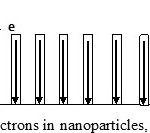 |
Figure 4: Movement of electrons in nanoparticles, Nanorods and nanotubes Click here to View figure |
1D Nanoarchitectures bear the potential to improve the weaknesses such as electron-hole recombination due to short charge transfer distances, and reactant adsorption and product desorption can be enhanced due to the high surface area. These also offer the opportunity to minimize the distances over which charges have to survive and be transported after excitation.
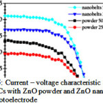 |
Figure 5: Current – voltage characteristic of DSSCs with ZnO powder and ZnO nanobelts as photoelectrode Click here to View figure |
However, a problem associated with discreet nanoparticles is that charges traveling between adjacent nanoparticles mainly through hopping process are neither efficient nor fast. Second, the high density of defects on the surface of nanoparticles, both crystallographic and electronic, acts as traps to hinder charge transport. To overcome these limitations, efforts have been made by researchers in the recent years. In thick film sample, excitations occurring at larger depths than the typical inelastic mean free path of electrons are useless to drive a surface reaction, thereby reducing the overall efficiency. So the quality and size of nanomaterial play a vital role in PEC splitting of water. There are many reports which show that nanorods, nanotubes, nanowires and quantum dots contribute significantly towards efficiency of the system as they offer high electrochemical charge transfer which in turn reduced the chances of photocorrosion and charge recombination. Zemin Zhang et al fabricated screw-like SnO2 nanostructure for PEC splitting of water by growing thread-like SnO2 nanosheets onto rod-like single-crystalline SnO2 nanowires28. The light absorption power of the screw-like SnO2 nanostructures was 33% higher than that of the pristine SnO2 nanowires. 1.3 % solar to hydrogen conversion efficiency have been reported by using Co doped ZnO nanowires29 while Weina Shi recorded 2.7 mA cm-2 at 0V (vs. RHE) with a maximum photon to current conversion efficiency of 0.28% at 0.21 V (vs . RHE) by using carbon coated Cu2O Nanowires30. Niyom reported Dye sensitized ZnO nanobelts showed maximum photocurrent compared to nanopowder (Fig 5.)31. Likewise Kwang also reported that high photocurrent was recorded with ZnO nanorods compared to Polycrystalline ZnO thin films32. The nanomaterials having large surface area provides high active sites for oxygen/hydrogen evolution at the electrode/solution interfaces. So the rise in photocurrent on using nanoarchitectures can be attributed to high surface area, superior carrier transport, low defect and reduced charge transfer distance.
Heterostructures
The absorption of solar spectrum by semiconductor material is the major factor determining the efficiency of the PEC system. Now a days research has been turned to improve the absorption power of the photoelectrode by combining semiconductor material with other material i.e.. nanocomposites, layered heterojunctions and doping33. These materials not only serves better absorption power but also reduced the recombination of charge carriers. Doping with metals and non metals is a very important technique to improve the overall efficiency. Pure semiconductors are generally highly resistive at room temperature, impurity doping is largely intended to improve electrical conduction either by raising the number of charge carriers and/or by increasing the carrier mobility of the material. The incorporation of Ru, Cu, Ni, Cr decreased the band gap of ZnO effectively by introducing intra band gap states and increased the efficiency of PEC system remarkably34,35. Sometimes these particles also serve as traps for charge carriers thereby reduced the recombination of charge carriers and results in enhance photocurrent12. There are various reports are available in which doping of S, N, Si, Ti, Cd, W etc significantly increased the efficiency of PEC system. These foreign particles not only introduces intraband gap states but also promotes charge transfer. Significant rise in photocurrent was recorded on incorporation of Cr3+ in the crystal lattice at the surface of α – Fe2O3 nanorod and this rise was attributed to high charge transfer36. Ti doped α-Fe2O3 synthsized by hydrothermal method offered photocurrent about 5.5 times compared to pristine Fe2O337. The introduction of Ti in crystal lattice of iron oxide decreased the charge transfer resistance. The Mott-schottky analysis shows that on doping chare carrier density increased from 3.39 x1016 cm-3 to 8.02 x1018 cm-3 suggesting high electrical conductivity. Xunyu Yang et al reported hydrogen generation efficiency of 0.15% by using Nitrogen doped ZnO nanowires (Fig 6)20. Cu2ZnSnS4 decorated TiO2 nanorods show high absorption power and when same material was combined with ZnS, the photocurrent density increased from 2.92 mA/cm2 to 6.91 mA/cm2 with efficiency 3.50%38. Recombination of charge carrier decreased significant on ZnS overlayering.
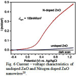 |
Figure 6: Current – voltage characteristics of undoped ZnO and Nitogen doped ZnO nanowires20 Click here to View figure |
Layered structures have also attracted the attention of researchers even with nanomaterials. A combination of small and large band gap material deposited one over the other may absorb full solar spectrum more efficiently. Basically small band gap material is used to sensitize the high band gap material via electron or hole injection by visible light absorption. If energy band edges match at the junction better and efficient separation of electron-hole is possible they offer considerably high photocatalytic activity on account of photogenerated electrons and holes van readily reaches the interlayer spaces of the reaction sites10. When two materials are combined, an internal electrical field is generated and reduced the electron – hole recombination. When the light shines the low band gap material, electron and holes are generated. The electrons thus produced are injected into the conduction band of core material and transferred to cathode by back contact to produce hydrogen (Fig 7). The sensitization of one material with another material may serve to absorb full solar spectrum. Overlayering not only facilitates charge transfer but also stabilize the underlying material39. Coating of thin shell of one over other layer deactivate surface states through removal of the hole traps, without affecting the minority carrier diffusion resulting in improved PEC performance. Yuangang recorded the photocurrent density of 1 mA/cm2 by using Fe2O3/WO3 as a photoelectrode which was 50 times more than that of pure Fe2O3 and this system was quite stable yielding 65% of initial current after 5 hours continuous illumination40. High photoresponse was recorded with Zinc Oxide Nanowire Photoanodes with Ultrathin Titania Shells due to passivation of surface states through removal of deep hole traps39. The flat band potential which is a key factor of PEC splitting of water can also be modified by using layered oxides because one oxide can occupy the surface states of other resulting in increased photoresponse41.
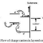 |
Figure 7: Flow of charge carriers in layered oxides Click here to View figure |
Core – shell made by embedding metal nanoparticles in semiconductor material offers better response as it reduce recombination of charge carriers by forming an energy barrier and also increase the porosity. As the porosity increases, contact between dye and material increases which in turn increases the efficiency of the system. Kai synthesized Er2O3@ZnO coreshell nanorods and applied them as a photoelectrode for PEC splitting of water42. Photocurrent density of 3.8 mA/cm2 was recorded which is significantly higher than the ZnO thin film. Mott–Schottky analysis shows that the charge carrier density of Er2O3@ZnO coreshell increases to 2.44 × 1018cm-3 from 1.24 × 1016cm−3 of ZnO. So the rise in photocurrent density was due to increase in charge carrier density and low charge recombination. Surface Modification The efficiency of PEC system depends on the absorption of light (Visible portion of light), charge transfer and stability in aqueous medium. Therefore many techniques have been applied to improve the visible light responsive semiconductors. Surface modification can be effective tool to modify the material properties for enhancement of photoresponse resulting in high current generation for splitting of water. Dot decoration Generally metals have positive oxidation state so they have tendency to accept the electron and this tendency sometimes become beneficial for PEC system. When the metal atom is deposited on semiconductor surface, they act as a sink for photogenerated electron and thus the chances of recombination of electrons and holes reduced which in turn increase the efficiency (Fig 8).
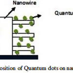 |
Figure 8: Deposition of Quantum dots on nanostructure |
Also these metal atoms reduced the band gap of material. A system having Zn dot on the surface of Zn doped hematite thin film was found to be exhibit much better PEC response as compared to doping or overlayering. Saroj et al deposited Zn dots of varying size ranging from 100 Å to 260 Å(Fig 9.).
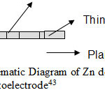 |
Figure 9: Schematic Diagram of Zn doted Fe2O3 Photoelectrode43 Click here to View figure |
Highest current was recorded with 230 Å but on moving towards big size, current density decreased may be due to interdiffusion of Zn inside the hematite near the interface (Fig 10.).
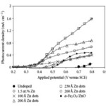 |
Figure 10 Click here to View figure |
Dotting of metal on surface may shift the band edge positions and acts as a catalyst for charge transfer reaction43. CdS quantum dots decorated screw like SnO2 nanostructure showed yielded photocurrent density of 9.9 mA/cm2 producing 159.6μmol (h cm2)-1 hydrogen. This rise in photocurrent was attributed to high charge transfer, better absorption power and larger surface area. CdS has low band gap material and absorbs visible light and on illumination the photoexcited electron is transferred to wide band gap material. The photocurrent density of 5.5 mA/cm2 has been recorded with CdS dotted TiO2 wothout any external bias44. Chih also reported that PbS decorated Al doped ZnO showed strong optical absorption in visible portion resulting in high photocurrent density45. Photoconversion efficiency of 0.63% was offered by TiO2 nanotube array modified with carbon nitride quantum dots46. These modifications not only increase the absorption of light but also suppress the charge recombination. So it can conclude that dot decoration of small band gap material on wide band gap nanostrcutres may be a effective tool to use the broad spectrum yielding high photon to current efficiency. Swift Heavy Ion Irradiation Swift heavy ion irradiation (energetic ions) can modify the surface as well as physico-chemical properties of the material as it can induce wide variety of defects in the material47. When these energetic ions strikes on materials it can result in defect creation, annealing, recrystallization or phase transition. It also cause redistribution of particle and increases the porosity. As the porosity increases, surface area for reaction increases which results in high photorespnse. High photocurrent (0.16 mA/cm2) with photon –current efficiency 0.91% was recorded by using BaTiO3 thin film irradiated by 120 MeV Ag9+ ions while photocurrent of 0.16 mA/cm2 was recorded by using SrTiO3 irradiated by same energetic ion48.
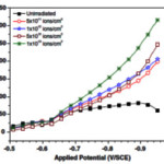 |
Figure 11 |
Fe2O3 thin films irradiated by 100 MeV Si7+ ions at fluence 2×10¹³ ions/cm2 exhibited better photoresponse compared to unirradiated film49 while TiO2 thin films, upon irradiation with 120MeV-Ag9+ exhibited a remarkable increase in photocurrent (0.76mA/cm2 at zero bias) relative to an unirradiated sample50. Irradiation of material with energetic ions can induce morphological and structural changes resulting in improved optical absorption, charge separation and donor density. However, this technique need to be optimised as the effect of SHI irradiation depends on the ion energy, fluence, temperature, and ion species51. Dye Sensitization The wide band gap materials are best suited for splitting of water but they do not absorb sunlight. So to overcome this problem, the dye sensitization of material is emerging as a favourite alternative to make an ideal system. During light irradiation, dye becomes photo-excited and injects electrons into the conduction band of semiconductor.
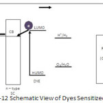 |
Figure 12: Schematic View of Dyes Sensitized |
Through the metal oxide film, electrons reach to the conducting substrate and by a back contact transfer to an external circuit to the counter electrode (Fig 12.). Working electrode (photoelectrode) plays an important role in charge collection and transportation of photo-excited electron from dye to external circuit. To obtain better photoresponse, HOMO and LUMO of dye must be in proper alignment with electron – hole quasi Fermi level of semiconductor and redox level of O2 and H252. ZnO thin film sensitized by crystal violet offered 5.8 mA/cm2 current density which is 347% higher than the current recorded with unsensitized ZnO53 while power conversion efficiency of 13% with current density 18.1 mA/cm2 has been recorded with engineered porphyrin dye sensitized TiO2 under full sun illumination54. Dye sensitized flower like 3D microstructure of TiO2 offered very high open circuit potential (0.84 V) but low power conversion efficiency (PCE) compared to nanoparticles. High crystal quality of microstructure offered better open circuit potential but due to low surface area current reduced55. To achieve a better power conversion efficiency, interfacial charge transfer plays a very important role. Very low dimensional particles face a problem of charge recombination due to large internal surface and low band banding. To reduce the recombination, core-shell structure may be used which forms a schottky barrier at electrode-electrolyte interface. However, in metal-semiconductor combination, concentration of metal must be optimized otherwise these metal may act as recombination centre at higher concentration56. The surface morphology, composition of semiconductor, band gap, thickness of semiconductor and microstructure and adsorption of dye on surface affects the overall efficiency of dye sensitized solar cell. However, the selection of dye, dye loading time and selection of electrolyte57 is also very important. Chemically modification of surface can also help to increase the efficiency of dye sensitized cells. Acetate modified TiO2 sensitized by N719 dye showed much better photoresponse compared to unmodified TiO2 and efficiency of such system was 5.3%58. Dye not only contributes to absorption of visible light but also suppresses the charge recombination and act as effective stabilizer. To improve the efficiency of dye sensitized solar cell, co-adsorbent can be apply to the system. A light-scattering cyanobiphenyl derivative 6-[(4′-cyano(1,1′-biphenyl)-4-yl)oxy]he-xanoic acid (CBHA) applied as co-adsorbent for dye sensitized cell increased the efficiency of the system by 0.81%59. Another approach to increase the efficiency is loading of semiconductor by metal like Ag, Au, Pt as they act as co-catalyst. On metal loading Schottky barrier is formed between metal nanoparticle and conduction band of semiconductor and thus thus permits fast electron injection58. Conclusion To face the energy crisis, PEC splitting of water may be the best solution. To implement this technique on commercial level, the conversion efficiency of PEC system must be around 10%. The efficiency of PEC system depends mainly on absorption of light, charge separation, charge mobility and band edge alignment. So to improve the efficiency of the system various strategies have been adopted by different researchers and work is going on. Nanotechnology can be used as a tool to tailor out the properties of material at microscopical level. Dye sensitization , surface modifications and doping are other imperative tool to find out the desired material. However, selection of photosensitive material is more important in this respect.
References
- http://www.indiaenergyportal.org/overview_detail.php
- BP Statistical Review of World Energy, June 2015
- Seyed, E. H.; Mazlan, A. W.; Renewable and Sustainable Energy Reviews, 2016,57, 850-866.
CrossRef - US DOE Hydrogen Program 2000 Annual Review, May 9-11, 2000, San Ramon, California
- Al-Amin, A. Q.; Ambrose, A. F.; Masud, M. M.; Azam, M. N.; International Journal of Hydrogen Energy, 2016,41, 42117-2127.
CrossRef - Belz, S.; Acta Astronautica, 2016, 121, 323-331.
CrossRef - Chen, S.; Thind, S. S.; Chen, A.; Electrochemistry Communications, 2016, 63, 10-17.
CrossRef - Zahedi, S.; Sales, D.; Romero, L. I.; Solera, R.; Bioresource Technology, 2013, 129, 85-91.
CrossRef - Singh, L.; Wahid, Z. A.; Journal of Industrial and Engineering Chemistry, 2015, 21, 70-80.
CrossRef - Choudhary, S.; Upadhyay, S.; Kumar, P.; Singh, N.; Satsangi, V R.; Shrivastav, R.; Dass, S.; International Journal of Hydrogen Energy, 2012, 37, 18713-18730.
CrossRef - Fujishima, A.; Honda, K.; Nature, 1972, 238, 37-38.
CrossRef - Li, Y.; Zhang, J. Z.; Laser and Photon. Rev, 2009, 1-12.
- Shrivastav, R.; Gupta, M.; Sharma, V.; Kumar, P.; Shrivastava, J.; Solanki, A.; Int. J. Nanoparticles, 2011, 4, 248-267.
CrossRef - Wang, D.; Zhang, X.; Sun, P.; Lu, S.; Wang, L.; Wang, C.; Liu, Y.; Electrochimica Acta, 2014, 130, 290-295.
CrossRef - Gupta, M.; Sharma, V.; Shrivastava, J.; Solanki, A.; Singh, A. P.; Satsangi, V. R.; Dass, S.; Shrivastav R.; Bulletin of Materials Science, 2009, 32, 23-30.
CrossRef - Huang, M. C.; Chang, W. S..; Lin, J. C..; Chang, Y. H.; Wu, C. C.;, Journal of Alloys and Compounds, 2015, 636, 176-182.
CrossRef - Ma, Q. B.; Hofmann, J. P.; Litke, A.; Hensen, E. J. M.; Solar Energy Materials and Solar Cells, 2015, 141, 178-186.
CrossRef - Xie, R.; Su, J.; Li, M.; Guo, L.; International Journal of Photoenergy, 2013, 2013, Article ID 620134, 1-7.
- Guo, M.; Wang, L.; Xia, Y.; Huang, W.; Li, Z.; International Journal of Hydrogen Energy, 2016, 41, 2278-2284.
CrossRef - Yang, X.; Wolcott, A.; Wang, G.; Sobo, A.; Fitzmorris, R. C.; Qian, F.; Zhang, J. Z.; Li, Y.; Nano letters, 2009; 9; 2331-2336
CrossRef - Tang, Y.; Rong Liu F.; Chu, M.; Dong, H.; Zhang, Y.; Xiao, P.; Applied Surface Science, 2016, 361, 133-140.
CrossRef - Monfort, O.; Pop, L. C.; Sfaelou, S.; Plecenik, T.; Roch, T.; Dracopoulos, V.; Stathatos, E.; Plesch, G.; Lianos, P.; Chemical Engineering Journal, 2016, 286, 91-97.
CrossRef - Fu, H.; Lin, J.; Zhang, L.; Zhu, Y.; Applied Catalysis A: General; 2006, 306, 58-67.
CrossRef - Xu, W.; Zheng, C.; Hua, H.; Yang, Q.; Chen, L.; Xi, Y.; Hu, C.; Applied Surface Science, 2015, 327, 140-148.
CrossRef - Bak, T.; Nowotny, J.; Rekas, M.; Sorrell, C. C.; International Journal of Hydrogen Energy, 2002, 27, 991-1022.
CrossRef - Lin, Y.; Yuan, G.; Liu, R.; Zhou, S.; Sheehan, S. W.; Wang, D.; Chemical Physics Letters, 2011, 507, 209-215.
CrossRef - Li, Z.; Feng, J.; Yan, S.; Zou, Z.; Nano Today, 2015, 10, 468-486.
CrossRef - Zhang, Z.; Gao, C.; Wu, Z.; Han, W.; Wang, Y.; Fu, W.; Li, X.; Xie, E.; Nano Energy; 2016, 19, 318-327.
CrossRef - Patel, P. P.; Hanumantha, P. J.; Velikokhatnyi, O. I.; Datta, M. K.; Hong, D.; Gattu, B.; Poston, J. A.; Manivannan, A.; Kumta, P. N.; Journal of Power Sources, 2015, 299, 11-24
CrossRef - Shi, W.; Zhang, X,; Li, S.; Zhang, B.; Wang, M.; Shen, Y.; Applied Surface Science, 2015, 358, 404-411.
CrossRef - Hongsith, N.; Choopun, S.; Chiang Mai J. Sci., 2010, 37, 48-54.
- Ahn, K. S.; Shet, S.; Deutsch, T.; Jiang, C. S.; Yan, Y.; Jassim, M. A.; Turner, J.; Journal of Power Sources, 2008, 176, 387-392.
CrossRef - Shen, S.; Chen, J.; Cai, L.; Ren, F.; Guo, L.; Journal of Materiomics, 2015, 1, 134-145.
CrossRef - Sharma, V.; Kumar, P.; Shrivastava, J.; Solanki, A.; Satsangi, V..R.; Dass, S.; Shrivastav, R.; International Journal of Hydrogen Energy, 2011, 36; 4280-4290
CrossRef - Sharma, V.; Kumar, P.; Singh, N.; Upadhyay, S.; Satsangi, V. R.; Dass, S, Shrivastav, R; International Journal of Hydrogen Energy, 2012, 37, 12138-12149.
CrossRef - Mao, S. S.; Shen, S.; Guo, L.; Progress in Natural Science: Materials International, 2012, 22, 522-534.
CrossRef - Chen, Y. J.; Chen, L. Y.; Energy Procedia, 2014, 61, 2046-2049
CrossRef - Ho, T. Y.; Chen, L. Y.; Energy Procedia, 2014, 61, 2050 – 2053.
CrossRef - Liu, M.; Nam, C. Y.; Black, C. T.; Kamcev, J.; Zhang L. .; J.Phys.Chem, 2013, 117, 13396−13402.
- Li, Y.; Feng, J.; Li, H.; Wei, X.; Wang, R.; Zhou, A.; International Journal of Hydrogen Energy, 2016, 41, 4096-4105.
CrossRef - Li, S. J.; Lin, Y.; Tan, W. W.; Zhang, J.; Zhou, X. W.; Chen, J. M.; Chen, Z.; Metallurgy and Materials, 2010; 17, 92-97.
- Ye, K. H.; Wang, J. Y.; Li, N.; Liu, Z. Q.; Guo, S. H.; Guo, Y. P.; Su, Y. Z.; Inorganic Chemistry Communications, 2014, 45, 116-119.
CrossRef - Kumari, S.; Singh, A. P.; Tripathi, C.; Chauhan, D.; Dass, S.; Shrivastav, R.; Gupta, V.; Sreenivas, K.; Satsangi, V R.; International Journal of Photoenergy, 2007; 2007 Article ID 87467, 1-6.
- Shin, K.; Yoo, J. B.; Park, J. H.; Journal of Power Sources, 2013, 225, 263-268.
CrossRef - Hsu, C. H.; Chen, C. H.; Chen, D. H.; Journal of Alloys and Compounds, 2013, 554, 45–50.
CrossRef - Su, J.; Geng, P.; Li, X.; Zhao, Q.; Quan, X.; Chen, G.; Nanoscale, 2015,7, 16282-16289.
CrossRef - Pattar, J.; Balakrishna, K. M.; Ganesh. S.; Mahesh, H.M.; Int. J. Thin Film Sci. Tec.; 2013; 2; 37-41.
- Solanki, A.; Shrivastava, J.; Upadhyay, S.; Choudhary, S.; Sharma, V.; Sharma, P.; Kumar, P.; Kumar, P.; Ehrman, S.; Satsangi, V. R.; Shrivastav, R.; Dass, S.; Current Applied Physics, 2013, 13, 344-350
CrossRef - Singh, A. P.; Tripathi, A.; Shrivastav, R.; Dass, S.; Satsangi, V. R.; Proc. of SPIE, 2008, 70440H.
CrossRef - Singh, A. P.; Kumari, S.; Tripathi, A.; Singh, F.; Gaskell, K. J.; Shrivastav, R.; Dass, S, Ehrman, S. H.; Satsangi, V. R.; J. Phys. Chem. C, 2010, 114, 622–626
CrossRef - Singh, A. P.; Kumari, S.; Shrivastav, R.; Dass, S.; Satsangi, V. R.; J. Phys. D: Appl. Phys., 2009, 42, 085303-085307.
CrossRef - Sengupta, D.; Das, P.; Mondal, B.; Mukherjee, K.; Renewable and Sustainable Energy Reviews, 2016, 60, 356-376.
CrossRef - Shrivastav, R.; Gupta, M.; Sharma, V.; Kumar, P.; Shrivastava, J.; Solanki, A.; Int. J. Nanoparticles, 2011, 4, 248-267.
CrossRef - Mathew, S.; Yella, A.; Gao, P.; Baker, R. H.; Curchod, B. F. E.; Astani, N. A.; Tavernelli, I.; Rothlisberger, U.; Nazeeruddin, M. K.; Gratzel, M.; Nature Chemistry, 2014, 6, 242–247
CrossRef - Que, Y. P.; Weng, J.; Hu, L. H.; Wu, J. H.; Dai, S. Y.; Journal of Power Sources, 2016, 307, 138-145.
CrossRef - Pandikumar, A.; Lim, S. P.; Jayabal, S.; Huang, N. M.; Lim, H. N.; Ramaraj, R.; Renewable and Sustainable Energy Reviews, 2016, 60, 408-420.
CrossRef - Singh, A.; Mohan, D.; Ahlawat, D. S.; Richa; Oriental Journal of Chemistry, 2016, 32 (2), 1049-1054
CrossRef - Lu, S.; Sun, S. S.; Geng, R.; Gao, J.; Thin Solid Films, 2015, 589, 8-12.
CrossRef - Wang, Y.; Sun, P.; Zhao, J.; Gao, M.; Yi, Q.; Su, Y.; Gao, L.; Zou, G.; Electrochimica Acta, 2016, 194, 67-73.
CrossRef

This work is licensed under a Creative Commons Attribution 4.0 International License.
About The Author
![]()
A New Edition of Web of Science
Journal Impact Factor
2022: 0.5
Five Year: 0.8
Journal is Indexed in

Cabells Whitelist
![]()


