Efficiency Investigation of Dye-Sensitized Solar Cells Based on the Zinc Oxide Nanowires
Ahmad Afifi1, Mohammad Kazem Tabatabaei2
1MUT- Department of Electrical Engineering, Tehran, Iran
2AUT-Department of Electrical Engineering, Tehran, Iran
DOI : http://dx.doi.org/10.13005/ojc/300118
Article Received on : September 18, 2013
Article Accepted on : November 08, 2013
Article Published : 06 Feb 2014
In this paper, we synthesized ZnO nanowires in dye sensitized solar cells. The nanowires have been fabricated using fast-microwave-hydrothermal process.We verify the effects of different lengths of ZnO nanowires on efficiency and absorptionofdye sensitized solar cells. J–V curves of the fabricated ZnO nanowire-based mercurochrome-sensitized solar cellsindicated that the short-circuit current density wouldincrease with increasing the length of nanowires.We also fabricate more efficient N719-sensitized solar cellsand investigate the effect of different length of Zno nanowires on the efficiency.
KEYWORDS:Zinc Oxide; nanowire; solar cell; Dye-sensitized; efficiency
Download this article as:| Copy the following to cite this article: Afifi A, Tabatabaei M. K. Efficiency Investigation of Dye-Sensitized Solar Cells Based on the Zinc Oxide Nanowires. Orient J Chem 2014;30(1) |
| Copy the following to cite this URL: Afifi A, Tabatabaei M. K. Efficiency Investigation of Dye-Sensitized Solar Cells Based on the Zinc Oxide Nanowires.. Orient J Chem 2014;30(1). Available from: http://www.orientjchem.org/?p=2024 |
INTRODUCTION
Third generation of solar cells is thin-film dye-sensitized with different layers on a substrate like a glass.Among different types of thin–film solar cells,because of their higher efficiency per production costratio compared to the other types of solar cells, dye-sensitizedsolar cells(DSSC) have been of great interest, recently(1-4).Most current researches in the field of dye-sensitized solar cells are on the light-absorbing of dye, improvement of stability of solar cell by replacing the electrolyte liquid cells with solid polymer ionic and electron transport in solar cell by high band gap semiconductors.The solutions seeking to increase the absorptionsurface,improve electron transfer and reduce electron recombination(5-7).
In recent years,due to their unique optical, chemical,electrical and piezoelectric properties,ZnO nanostructureshave become very common in semiconductor devices(8-14). ZnO nanowiresin a dye-
sensitized solar cell create a direct electron pathwaywhich leads to an increase in electron diffusion length andlifetime.Several methods such as vapor–liquid–solid, metal–organic chemical vapor deposition and thermal evaporation (5, 15) have been introduced in order to grow a high quality ZnO nanostructure array at high temperatures. To make the growth process of ZnO nanostructures more energy efficient and cost-effective, the temperature of process should be reduced. Therefore, solution-based methods with the goal of low-cost ZnO nanostructure growth at low temperatures have been developed recently (5,16–18). Solution-based methods include a process called hydrothermal(18). Microwave-assisted hydrothermal method with the aim of rapid heating of the solution and thereby reducing the time needed for reaching the crystallization temperature in the growth environment has been tested and looks to be successful(17,18).A promising way to improve the efficiency of DSSC is
increasing the life time and diffusion length of electron by using of high band gap semiconductor arrays(19,20). In our investigation we fabricated long and vertically aligned Zno nanowire arrays to use in DSSC.
Fabrication Zno nanowire
Hydrothermalprocess consists of two parts. One is seeding a layer on a substrate and another growth of Zno nanowire, our proposed method, like in most of the other methods. Seed layer is the main part that affects the length and size of Zno nanowire(19, 24).In this research spin coating method was selected. Figure 1 indicates the schematic of seeding layer on glass substrate by spin-coating method. Before seeding layer on substrate, it is essential to clean it by deionized water and acetone.
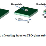 |
Fig.1: Schematic of seeding layer on ITO-glass substrate by spin-coating method. Click here to View Figure |
Deposition solution containinga 5 mM solution of zincacetate dihydrate in acetonemade at room temperature. To have uniform seed layer, speedof 2000 rpm for 60 s in spin-coating method was selected and was repeated five timesand then substrates were annealed in air at 350 ˚C for 20 min to decomposition of zinc acetate.
The ZnO nanowires were grown in a solution including25 mM zinc nitrate hexahydrate,12.5mM hexamethylenetetramine,5 mMpolyethylenimine and 0.8 M ammonium hydroxideinto 200 ml deionized water. Afterwardthewhole system was heated by microwave oven for different power levels and different time.
Design of dye-sensitized solar cells
Several lengths of Zno nanowire on an ITO- glass substrate werefabricated byproposed method which described in pervious section.array of Zno nanowire should be calcined at 450˚C for 1 hour because this action lead to improvement of dye absorption onto the arraysurface of Znonanowire and finally improvement of efficiency of DSSC.Figure 2 indicate the schematic of dye sensitized solar cell manufacture process.
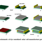 |
Fig.2: schematic of dye sensitized solar cell manufacture process. Click here to View Figure |
fabrication DSSCs process consist of seeding layer of zinc oxide on selective space of glass substrate which indicated on Figure 2-1, Figure 2-2 and Figure 2-4, then growth of Zno nanowire depicted on Figure 2-5 and Figure 2-6. The counter electrode wasprepared by spin coating method. A few drops of a 10 mM solution ofhexachloroplatinic acid hexahydrate(H2PtCl6.6H2O)in ethanol,dispensed on the conductive side of another ITO substrate whichis shown in Figure.2-7. The substrate was then annealed at 450˚C for 30 min. An insulation between the sensitized electrode and the platinized counter electrode is required which here a 50 µm thick hot melted double-layer parafilmis used. The electrolyte solutioninjected into the cell is0.3 M lithium iodide and 0.03 M iodine in acetonitrile as electrolyte solution.
The morphology of ZnO nanowire was characterized by SEM. Because the main goal of this paper is studying the effect of length of Zno nanowire on efficiency of solar cells, some cells by different length of ZnO nanowires were fabricated and characterized.
Results and discussion
Figure 3-1 indicates SEM image of Zno nanowire on glass substrate with a seed layer which seeding layer done by spin coating method. In most of the methods based on the hydrothermal process, seeding of the substrate surface before the growth of the nanowire is essential. Figure 3-2 showsZno nanowire grown on glass substrate that were seeded a layer twice by repeating spin coating method. By comparing the Figures repeating spin coating method cause uniform and narrow diameter distribution of Zno nanowires. In addition, nanowires are well aligned because of the increased seed layer thickness. Therefore, seeding the substrate twice using the spin-coating method seems to be the optimum approach for hydrothermal process.
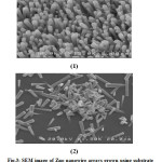 |
Fig.3: SEM image of Zno nanowire arrays grown using substrate seeding method: (1) spin coating (2) twice-performed spin coating Click here to View table |
We should reduce diameters and increment length of Zno nanowire to achievelarge internal surface area of the ZnO nanostructure in a highly effective agent to improve the separation of electrical charges in semiconductor devices(21)In conventional hydrothermal method we cannot achieve such structure. So, according other research ammonium hydroxide and polyethylenimine (PEI) can beadded to the growth solution to obtaining high aspect ratio (21).Long length and small diameter of the ZnO nanowires is clearly indicated in Figure 4.Figure 4 shows the SEM images of the longest possibleZnO nanowire arrays grown using the proposedmethod at different microwave power levels. The increase of the growth rateand the aspect ratio enhancement of the ZnO nanowiresby increasing the microwave power level are clearly visible in thisFigure. Cross-sectional SEM images revealed that the power level is proportional to the growth rate of the nanowires, which means increasing the power lengthens the nanowire arrays and reduces the growth process time.
During this investigation, Average length ofZno nanowires grown using different microwave power levels were considered. Figure 5shows the average longitudinal growth ofZnO nanowires versus growth process time for ourmethod at different microwave powerlevels. At growth times more than 10 min, for low microwave power levels, the longitudinal growth of ZnO nanowire continued its rising trend by increasing the process time and also this condition is the same when higher power level is applied.
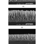 |
Fig.4: SEM images of the longest ZnO nanowires grown at different microwave power levels: (1) 180W 80 min (2) 450 W 50 min (3) 850 W 30 min, without any growth solution refreshment. Click here to View table |
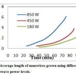 |
Fig.5:Average length of nanowires grown using different microwave power levels. Click here to View Figure |
For fabrication of DSSC, mercurochrome was used for sensitization of ZnO nanowires, because itis much cheaper than the Ru-based dyes and also provedto have better performance than the Ru-based N3 dye forZnO nanowire-basedsolar cellsDSSCs (23). For more investigation on efficiency and effect of length, N719 for sensitization of Zno nanowire was used.By comparing result of Figure 5 to other method like preferential (22) and rapid microwave assisted method (23) clearly demonstrate the advantage of this method and also obviously indicated that thismethod has a higher growth rate even at low power levels.
Table 1 show the summary of resultsfor short-circuits current density (JSC), open-circuit voltage(VOC), fill factor (FF) and power conversion efficiency (η) for mercurochrome-sensitized solar cell. And for more realization J-V of DSSC for different sample is shown in figure 6.The results of performance of DSSCs indicatedthat theefficiency of the DSSC is a function of increaseslength of the nanowire. Increment of length of Zno nanowire cause increase absorption dye on surface Zno nanowire and so increase efficiency of DSSC. A maximumefficiency of 0.79% was achieved in a DSSC prepared by a13µm long nanowire array, with short-circuit current densityof 4.96 mA/ cm2, open-circuit voltage of 0.43 V and fillfactor of 0.37.
Table.1:Summary of the performance results for ZnOnanowire DSSCs based on mercurochrome
|
Length of Zno nanowire arrays (µm) |
JSC (mA/cm2) | VOC (V) | FF | η (%) | ||
| 9 | 3.15 | 0.40 | 0.34 | 0.43 | ||
| 11 | 4.59 | 0.44 | 0.37 | 0.75 | ||
| 13 | 4.96 | 0.43 | 0.37 | 0.79 | ||
| 16 | 3.98 | 0.46 | 0.34 | 0.62 | ||
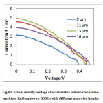 |
Fig.6:Current density–voltage characteristics ofmercurochrome-sensitized ZnO nanowire DSSCs with different nanowire lengths Click here to View table |
By comparing minimum and maximum efficiency the improvement in short-circuit current density is much larger than the open-circuit voltage is observed. So, efficiency of the cells seems to be mainly attributed to the increased short-circuit current density.Internal surface area of cell increased by increment of the length of Znonanowire array, which leads to the improved dye loading and it isthe main reason for the short-circuit current density increaseand, as a result, the power conversion efficiency enhancement.
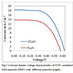 |
Fig.7 :Current density–voltage characteristics of N719 -sensitized ZnO nanowire DSSCs with different nanowire lengt Click here to View Figure |
It should be noted that the efficiency of N719-sensitized DSSCs is still much higher than that of mercurochrome-sensitized ZnOnanowire DSSCs.short-circuit current density of this cell is higher but the ratio of efficiency is about same. The reason of high efficiency could be the wider absorbance spectrum of the N719 dye than that of the mercurochromeand larger internal surface area for dye adsorption and to more efficiency of DSSC.
Tables 2 show the summary of resultsfor N719 -sensitized solar cell which indicate high efficiency. But changes of efficiency in the two cases are almost identical. And also figure 7 show photocurrent density versus voltage of N719 -sensitized solar cell. As expected, short current density is increased due to increment ofinternal surface area and dye adsorption.
Table.2:Summary of the performance results for ZnOnanowire DSSCs based on N719
|
Length of Zno nanowire arrays (µm) |
JSC (mA/cm2) | VOC (V) | FF | η (%) | ||
|
9 |
13.49 | 0.57 | 0.57 | 4.47 | ||
|
13 |
18.10 | 0.62 | 0.58 | 6.5 | ||
Conclusion
In this research, we fabricated vertically aligned Zno nanowire arrays by microwave hydrothermal process used for manufacturing dye sensitized solar cells. We grew several length of Zno nanowire by proposed method which has a higher growth rate in comparison with the other fast method and low power level. Experimental results clearly show that the efficiency of DSSC gradually increases with increasing length of nanowire arrays. Results show also thatincrement length of Zno nanowirescause increasing absorption of dye on surface ofZno nanowires.
References
- Plank N.O., Howard I.,Rao A., Wilson M.B., WellandM.E. and et.al, J. Phys. Chem. C.,113, 18515–22 (2009).
- Green M.A., J Mater Sci: Mater Electron.,18 ,15-19 (2007).
- Anta J.A. , GuillenE. and Tena-ZaeraR. , J. Phys. Chem. C., 116,11413–25 (2012).
- O’reganB. and GratzelM., Nature.,353, 737–40 (1991)
- Law M., Greene L. E., Johnson J. C., SaykallyR. andYang P., Nat Mater., 4,455-59 (2005).
- HoriuchiH. and et al., J. Phys. Chem. B., 107, 2570-74(2003).
- Wu J.J, Chen G.R, Yang H.H, Ku C.H. and Lai J.Y, Applied Physics Letters., 90, 213109 (2007).
- AryaS.K., SahaS., Ramirez Vick J.E., Gupta V., BhansaliS. and Singh S.P., AnalyticaChimicaActa., 737, 1– 21(2012).
- Wang J.X., Sun X.W., Yang Y., Huang H., Lee Y. C.,Tan O.K. and Vayssieres L., Nanotechnology., 17, 4995–8 (2006).
- Konenkamp R., Word R.C. and Schlegel C.Appl. Phys. Lett., 85, 6004–6 (2004).
- Goldberger J., Sirbuly D.J., Law M., and Yang P., J. Phys. Chem. B., 109, 9–14 (2005).
- Suehiro J., Nakagawa N., Hidaka S.I., Ueda M., Imasaka K., Higashihata M., Okada T. and Hara M.Nanotechnology., 17, 2567–73(2006).
- Wang Z.L. and Song J.H, Science., 312, 242–6 (2006).
- Law M., Greene L.E., Johnson J.C., Saykally R. and Yang P., Nature Mater., 4, 455–9 (2005).
- Stathatos E., LianosP., ZakeeruddinS., LiskaP. and GratzelM.,Chemistry of materials.15,1825–29 (2003).
- Greene L.E. andet.al.,AngewandteChemie International Edition. , 42, 3031-34 (2003).
- Greene L.E. and et al., Nano Lett., 5, 1231-36 (2005).
- UnalanH.E., HiralalP., RupesingheN., DalalS., Milne W.I. and Amaratunga G.A.J., Nanotechnology., 19, 255608 (2008).
- Benkstein K.D., KopidakisN., van de LagemaatJ. and Frank A.J., J. Phys. Chem. B.,107,7759-67 (2003).
- Yang P. and et al.,Advanced Functional Materials., 12, 323-31 (2002).
- Zhou Y., Wu W., Hu G., Wu H. andCui S., Materials Research Bulletin., 43, 2113–18 (2008).
- XuC., Shin P., Cao L.andGaoD., J. Phys. Chem. C., 114, 125-129(2009).
- Wu J.J., Chen G.R., Yang H.H., Ku C.H. and Lai J.Y., Appl. Phys. Lett., 90, 213109 (2007).
- Tabatabaee MK and Afifi A, Journal of American Science, 9(X) Accepted (2013).

This work is licensed under a Creative Commons Attribution 4.0 International License.
![]()
A New Edition of Web of Science
Journal Impact Factor
2022: 0.5
Five Year: 0.8
Journal is Indexed in

Cabells Whitelist
![]()


