The Potentiostatic Electrodeposition of Indium doped Aluminium Selenide Thin Films
R.K. Pathak and Sipi Mohan
Department of Chemistry, Holkar Science College, Indore (M.P.)
DOI : http://dx.doi.org/10.13005/ojc/290327
Article Received on :
Article Accepted on :
Article Published : 28 Oct 2013
The In containing AlSe thin films were electrosynthesized by electrochemical co-deposition technique. The morphological properties of thin films were studied through the Scanning Electron Micrograph (SEM) while the structural features through X-Ray Diffraction technique (XRD). The deposition current along with the film thickness values, the charge carrier density, flat band potential, corrosion characteristics i.e., corrosion current, corrosion potential and corrosion rate were calculated.
KEYWORDS:Potentiostatic Electrodeposition;Saturated Calomel Electrode (SCE);Scanning Electron Micrograph (SEM);X-Ray Diffraction (XRD);Charge Carrier Density (ND);Flat Band Potential (Efb);Corrosion Current (Icorr);Corrosion Potential (Vcorr) and Corrosion Rate (CR)
Download this article as:| Copy the following to cite this article: Pathak R. K, Mohan S. The Potentiostatic Electrodeposition of Indium doped Aluminium Selenide Thin Films. Orient J Chem 2013;29(3). doi : http://dx.doi.org/10.13005/ojc/290327 |
| Copy the following to cite this URL: Pathak R. K, Mohan S. The Potentiostatic Electrodeposition of Indium doped Aluminium Selenide Thin Films. Orient J Chem 2013;29(3). Available from: http://www.orientjchem.org/?p=314 |
Introduction
The In containing AlSe thin films have significance in various applications particularly in electronic devices. The electrodeposition of these films was carried out potentiostatically. Certain methods are performed for this purpose but here thin films were electrosynthesized by electrodeposition method1-14 which is considered as the simple, effective and cheap to obtain Aluminium chalcogenide thin films. The kinetics of electrode reactions was studied by I-t characteristics. The charge carrier density and flat band potential were determined by the capacitance measurement. With the help of I-t characteristics deposition current and film thickness were also determined. These films were characterized by Scanning Electron Micrograph (SEM) and structural features of these films were studied by X-Ray Diffraction technique (XRD). In order to study the corrosion characteristics of the films polarization techniques were used.
Result and Discussion
The electrodeposition of In doped AlSe thin films had been carried out at -0.700 mV vs SCE at room temperature. The current-potential behavior of AlSe was helpful to decide the deposition potential value. Fig. 1 shows the current-voltage behavior of AlSe solution. During the deposition of AlSe, the current decreases very fast upto a steady state values. Fig. 2 shows the variation of current with time for AlSe. These current-time characteristics were also studied for different compositions of In containing AlSe and AlIn thin films. The decrease in the current indicates the total coverage of the deposits on the surface of the substrate as well as the quality of the deposited material. The deposition current and the film thickness were also estimated by the amount of charge passed through the electrolyte. The deposition current and film thickness (ft) values are given in table 1. These values were also estimated for the different compositions of In containing AlSe thin films and AlIn. The film thickness value increases on the inclusion of In concentration.
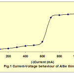 |
Fig. 1: Current Voltage behaviour of AISe thin film Click here to View figure |
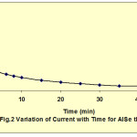 |
Fig. 2: Variation of Current with Time for AISe thin film Click here to View figure |
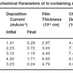 |
Table1: Electrochemical Parameters of In containing AlSe thin films Click here to View table |
The charge carrier density (ND) and the flat band potential (Efb) of these deposited films had also been studied with the help of Mott-Schottky plots15-20. Fig. 3 shows the Mott-Schottky plot for In containing AlSe film. The slope of these plots describes the ND while the extrapolation and intersection of these curves at potential axis determines the Efb. The values of ND and Efb are also shown in table 1 for all the compositions of AlSe, In containing AlSe and AlIn solutions. The charge carrier density values increases with increasing the concentration of Indium in the electroplating solution. The capacitance data indicates that the prepared films shows p-type semiconductor.
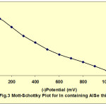 |
Fig. 3: Mott-Schottky plot for in containing AISe thin film Click here to View figure |
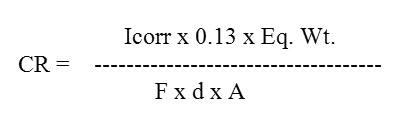
The polarization studies of the electrodeposited films had been carried out. The potential of the working electrode was varied with respect to SCE and corresponding current flowing between the working and counter electrode was measured to obtain Tafel Plots. In order to improve the resistance of the electrodeposited thin films against corrosion the inhibitor Benzotriazole was added to the electrolyte. The corrosion characteristics21-24 had also been studied in the presence of inhibitor. Fig. 4 shows the tafel plot for 0.006M In containing AlSe thin film in the absence and in the presence of inhibitor. With the help of these tafel plots Icorr and Vcorr were estimated while the CR was calculated with the help of an expression:
Where,
Icorr = Corrosion Current of the deposited film.
Eq.Wt. = Equivalent Weight of AlSe.
F = Faraday’s Constant.
D = Density of AlSe.
A = Area of the substrate.
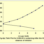 |
Fig. 4(a): Tafel Plot for 0.006 M in containing AISe thin film in absence of inhibitor Click here to View figure |
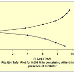 |
Fig. 4(b): Tafel Plot for 0.006 M in containing AISe thin film in presence of inhibitor Click here to View figure |
These tafel plots were constructed for AlSe, In containing AlSe from 0.002 M to 0.006 M concentration and AlIn thin films, in the absence and in the presence of inhibitor. Table 2 shows the values of Icorr, Vcorr and CR in the absence and in the presence of inhibitor. These data shows that the values of Icorr and CR increases while Vcorr decreases with the increment of In in AlSe solution in absence and in presence of inhibitor.
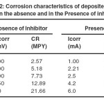 |
Table2: Corrosion characteristics of deposited thin films in the absence and in the Presence of inhibitor Click here to View table |
Scanning Electron Micrograph (SEM) is the source of studying the surface morphology of the deposited films25-30. Fig. 5 shows the SEM of the electrodeposited (a) AlSe (b) 0.004 M In containing AlSe and (c) AlIn thin films respectively. The increment of Indium in different compositions in the electroplating solution affects the morphology of the films. The particle size of the deposited films range from 100 nm to 400 nm. The change in the particle size also supports the fact that there is an addition of Indium in different concentrations in the electroplating solution. The surface of the film shows the continuity and homogeneity.
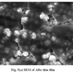 |
Fig. 5(a): SEM of AlSe thin film Click here to View figure |
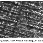 |
Fig. 5(b): SEM of 0.004 M In containing AlSe thin film Click here to View table |
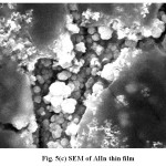 |
Fig. 5(c): SEM of AlIn thin film Click here to View table |
The crystallite size of the deposited films was studied by X-Ray diffraction method31-36 (XRD) using Scherrer’s formula,
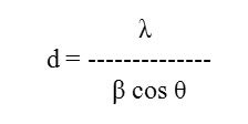
Where,
λ = Wavelength used 1.5418 Aº
β = Angular line width at half maximum intensity in radians
θ = Bragg’s angle
grain size was found to be of the order of ~ 26nm in AlSe, ~ 22nm in In containing AlSe and ~42 nm in AlIn.
Fig. 6(a), 6(b) and 6(c) shows XRD pattern of AlSe, 0.004M In containing AlSe and AlIn thin films by SILAR method. Comparison of d-values with ASTM data for AlSe shows that the material is AlSe having hexagonal structure.
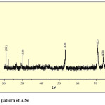 |
Fig. 6(a): XRD pattern of AlSe Click here to View table |
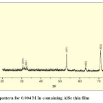 |
Fig. 6(b): XRD pattern for 0.004 M In containing AlSe thin film Click here to View table |
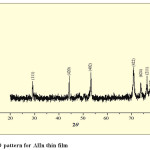 |
Fig. 6(c): XRD pattern for AlIn thin film Click here to View table |
Experimental Method
The In doped AlSe thin films have been electrosynthesized at -0.700 mV vs SCE at room temperature. The starting materials were 0.01 M AlK(SO4)2 (Sd fine), 0.01 M SeO2 (Sd fine) and 0.001 M InCl3 (Sd fine). Among these materials, the concentrations of AlK(SO4)2 and SeO2 were kept constant through out the experiment and the concentration of InCl3 was varied from 0.002 M to 0.006 M. Different compositions of In were added in the total concentration of AlSe solution. Thus, five electrodes were prepared for each concentration of In in AlSe.
Two Ti plates were used among which one was used as working electrode, another as counter electrode and SCE as reference electrode. All the three electrodes were dipped in electrolyte for some time in order to attain the state of equilibrium. The deposition of electrode was carried out for one hour. The deposited films obtained were then investigated under different parameters. The corrosion characteristics of these deposited films were determined. For this determination, the redox solution AlK(SO4)2 and KI/I2 was prepared. The deposited films were dipped in this redox solution to test the corrosion parameters in absence and in presence of inhibitor. Tafel plots were also constructed to determine the Icorr, Vcorr and CR. The capacitance of the films was measured by the LCR meter (systronic). The characterization of these deposited films was done with the help of SEM and the structural features were determined with the help of XRD.
Acknowledgement
The author is extremely grateful to the Principal and Head of the Chemistry Department Holkar Science College, Indore for their encouragement and co-operation. Our sincere thanks to the Director, UGC-DAE, Indore for providing SEM and XRD facility. Also thanks to Mr. V.K. Ahire and Mr. Ram Chaudhary for their guidance.
References
- Soon Hyung Kang, Yu-Kyung Kim, Don-Soo Choi and Yung-Eun Sung, Electrochimica Acta, 512, 2006, 14433-4438.
- A. Goetzberger, and C. Hebling, Sol. Energy Mater. Sol. Cells, 62, 2000, 1-19.
- M.A. Green, K. Emery, D.L. King, S. Igari, and W. Warta, Prog. Photovolt.: Res. Appl., 9, 2002, 55-61.
- S. Siebentritt, Thin Solid Films, 403-404, 2002, 1-8.
- D. Schmid, M. Ruckh, F. Grunwald, and H.W. Schock, J. Appl. Phys., 73, 1993, 2902-2909.
- R. Klenk, Thin Solid Films, 387, 2001, 135-140.
- Dhananjay, J. Nagaraju and S.B. Krupanidhi, Materials Science and Engineering: B, 127 (1), 2006, 12-16.
- U. Rau, A. Jasenek, H.W. Schock, F. Engelhardt, and Th. Meyer, Thin Solid Films, 361-362, 2000, 298-302.
- Ming-Zhe Xue and Zheng-Wen Fu, Thin Solid Films, 516 (23), 2008, 8386-8392.
- G. Hanna, A. Jasenek, U. Rau, and H.W. Schock, Thin Solid Films, 387, 2001, 71-73.
- T. Dullweber, O. Lundberg, J. Malmström, M. Bodegård, L. Stolt, U. Rau, H.W. Schock, and J.H. Werner, Thin Solid Films, 387, 2001, 11-13.
- T. Dullweber, G. Hanna, W. Shams-Kolahi, A. Schwartzlander, M.A. Contreras, R. Noufi, H. W. Schock, Thin Solid Films, 361-362 (2000) 478-481.
- T. Wada, N. Kohara, S. Nishiwaki, and T. Negami, Thin Solid Films, 387 (2001) 118-122.
- T. Nakada, T. Kume, T. Mise, and A. Kunioka, Jpn. J. Appl. Phys., 37 (1998) L499-L501.
- F.-J. Haug, D. Rudmann, G. Bilger, H. Zogg, and A.N. Tiwari, Thin Solid Films, 403-404 (2002) 293-296.
- Kato Tatsuya, Yamanashi Hidenori, Eto Akihiro, Kando Masashi, Reports of the Graduate School of Electronic Science and Technology, 21, 2000, 69-74.
- A. Jasenek, U.Rau, K. Weinert, I.M. Kötschau, G. Hanna, G. Voorwinden, M. Powalla, H.W. Schock, and J.H. Werner, Thin Solid Films, 387, 2001, 228- 230.
- A. Jasenek, and U. Rau, J. Appl. Phys., 90, 2001, 650-658.
- M. Köntges, R. Reineke-Koch, P. Nollet, J. Beier, R. Schäffler, and J. Parisi, Thin Solid Films, 403-404, 2002, 280-286.
- M. Bodegård, K. Granath, and L. Stolt, Thin Solid Films, 361-362, 2000, 9-16.
- N.W.Khun, E.Liu and X.T.Zeng, Corrosion Science, 51 (9), 2009, 2158-2164.
- Rishi Sharma, P.K. Barhai and Neelam Kumari, Thin Solid Films,516 (16), 2008, 5397-5403.
- M.E. Soares, C.A.C. Souza and S.E. Kuri, Surface and Coatings Technology, 201 (6), 2006, 2953-2959.
- Y. Gao, Z. J. Zheng, M. Zhu and C. P. Luo, Materials Science and Engineering A, 381 (1-2), 2004, 98-103.
- M. Lammer, U. Klemm, and M. Powalla, Thin Solid Films, 387, 2001, 33-36.
- A. Meeder, L. Weinhardt, R. Stresing, D. Fuertes Marrón, R. Würz, S. M. Babu, T. Schedel-Niedrig, M. Ch. Lux-Steiner, C. Heske and E. Umbach, Journal of Physics and Chemistry of Solids, 64 (9-10), 2003, 1553-1557.
- U. Rau, and H.W. Schock, Appl. Phys. A: Mater. Sci. Process., 69, 1999, 131-147
- A. Rockett, J.S. Britt, T. Gillespie, C. Marshall, M.M. Al Jassim, F. Hasoon, R. Matson, and B. Başol, Thin Solid Films, 372, 2000, 212-217.
- S.-H. Wei, S.B. Zhang, and A. Zunger, J. Appl. Phys., 85, 1999, 7214-7218.
- M.A. Contreras, B. Egaas, D. King, A. Schwartzlander, and T. Dullweber, Thin Solid Films, 361-362, 2000, 167-171.
- R. Caballero, and C. Guillén, Thin Solid Films, 403-404, 2002, 107-111.
- M. Klenk, O. Schenker, V. Alberts, and E. Bucher, Semicond. Sci. Technol., 17, 2002, 435-439.
- D. W. Lane, K. D. Rogers, J. D. Painter, D. A. Wood and M. E. Ozsan, Thin Solid Films 361-362, 2000, 1-8
- J.M. Merino, S. Mahanty, M. LeoÂn, R. Diaz, F. Rueda, J.L. Martin de Vidales, Thin Solid Films, 361-362, 2000, 70-73.
- Kong-Wei Cheng, Chao-Ming Huang, Guan-Ting Pan, Wen-Sheng Chang, Tai-Chou Leeand Thomas C.K. Yang, Journal of Photochemistry and PhotobiologyA:Chemistry, 190 (1), 2007, 77-87.
- S. Zein El Abedin, A.Y. Saad, H.K. Farag, N. Borisenko, Q.X. Liu and F. Endres, Electrochimica Acta, 52 (8), 2007, 2746-2754.

This work is licensed under a Creative Commons Attribution 4.0 International License.
![]()
A New Edition of Web of Science
Journal Impact Factor
2022: 0.5
Five Year: 0.8
Journal is Indexed in

Cabells Whitelist
![]()


