Performance Evaluation of ZnO based Rare Earth Element Doped Thin Films
Manish Sharma1*, R.P. Gairola2
*1Department of Physics, Govt. College Dhaliara-177103 (H.P.), India. 2Department of Physics, H.N.B Garhwal (Central) University, Srinagar, Uttarakhand, India
DOI : http://dx.doi.org/10.13005/ojc/290323
Article Received on :
Article Accepted on :
Article Published : 28 Oct 2013
In DMS materials, a small fraction of a host semiconductor cation is substituted by magnetic ions. We chose as semiconducting host the transparent ZnO, with a bandgap of 3.3 eV at room temperature. Studies on ZnO doped with 3d transition metals indicated only small magnetic moments. The more recent results for Gd in GaN, indicating high magnetic moments, motivated us to investigate ZnO thin films doped with rare earth (RE) metal ions. For the 3d transition metals, the 3d electrons are exterior and delocalized; leading to strong direct exchange interactions and high Curie temperatures, but often the orbital momentum is zero, leading to small total magnetic moments per atom. In RE metals, the 4f electrons are localized, exchange interactions are indirect, via 5d or 6s conduction electrons, but the high orbital momentum is leading to high total magnetic moments per atom, like 3.27μB for Nd. The Curie point for Nd is 19 K. In this paper we present the results of our study on ZnO films doped with Nd. Hall measurements are performed to investigate the electrical properties of films. Here we prepared and investigated ZnO films doped with different concentration of Nd. The films are grown on a-plane Al2O3 or SiO2 substrates. Hall investigations of electrical properties revealed the presence of a degenerate, highly conducting, film–substrate interface layer for the films grown on Al2O3; such an effect can be avoided, for example, by using SiO2 substrates. Magnetotransport measurements indicated no anomalous Hall effect, but a pronounced negative magneto resistance ratio that can be interpreted as a paramagnetic response of the system to the applied magnetic field. We would like to proceed with the surface sensitive techniques for investigating magnetic properties of ZnO:RE thin films.
KEYWORDS:Rare Earth;Thin Films;Hall measurements;Spinotronics
Download this article as:| Copy the following to cite this article: Sharma M, Gairola R P. Performance Evaluation of ZnO based Rare Earth Element Doped Thin Films. Orient J Chem 2013;29(3). doi : http://dx.doi.org/10.13005/ojc/290323 |
| Copy the following to cite this URL: Sharma M, Gairola R P. Performance Evaluation of ZnO based Rare Earth Element Doped Thin Films. Orient J Chem 2013;29(3). Available from: http://www.orientjchem.org/?p=304 |
Introducation
Since last two decades there has been an explosive growth of research in the field of thin films[1-3]. Several articles and books have been published on different aspects of elements doped thin films. These may be in the range of 10 to 1000 nm size and one can reduce the dimension in one, two or all three directions to obtain thin films, wires or dots, respectively. Note that these thin films can be of various shapes too and properties may change according to size and/or shape. One of today’s challenges for the development of future technologies is the realization of devices that control not only the electron charge, as in present electronics, but also its spin, setting the basis for future spintronics [4-5]. Spintronics represents the concept of the synergetic and multifunctional use of charge and spin dynamics of electrons, aiming to go beyond the semiconductor electronics and magnetic storage technology. The most direct method to induce spin-polarized electrons into a semiconductor is by introducing appropriate transition-metal or rare-earth dopants producing a dilute magnetic semiconductor (DMS). The DMS are semiconducting materials in which a fraction of the host cations can be substitutionally replaced by magnetic ions. These DMS are the building blocks of the future “Spintronics” devices.Hence we chose as semiconducting host the transparent ZnO, with a bandgap of 3.3 eV at room temperature. Studies on ZnO doped with 3d transition metals indicated only small magnetic moments [6–8]. The more recent results for Gd in GaN, indicating high magnetic moments [9], motivated us to investigate ZnO thin films doped with rare earth (RE) metal ions. For the 3d transition metals, the 3d electrons are exterior and delocalized, leading to strong direct exchange interactions and high Curie temperatures, but often the orbital momentum is zero, leading to small total magnetic moments per atom. In RE metals, the 4f electrons are localized, exchange interactions are indirect, via 5d or 6s conduction electrons, but the high orbital momentum is leading to high total magnetic moments per atom, like 3.27μB for Nd. The Curie point for Nd is 19 K.
In this paper we present the results of our study on ZnO films doped with Nd. Hall measurements were performed to investigate the electrical properties of films and they revealed a non-uniform distribution of the free electrons for the films grown on Al2O3. Magnetotransport measurements revealed a large negative magnetoresistance (MR) in ZnO films doped with RE metals.
Method
For the growth of RE alloyed ZnO Pulsed laser deposition (PLD) technique is used. Pulsed laser deposition (PLD) is a thin film deposition technique where a high power pulsed laser beam is focused inside a vacuum chamber to evaporate material from a target of the desired composition and deposited as thin film on a substrate. The physical phenomena of laser-target interaction and film growth are quite complex (form more details see reference [12–13]. The laser pulse is absorbed by the target and energy is first converted to electronic excitation and later on into thermal, chemical and mechanical energy, which result in evaporation, ablation and plasma formation [14]. The ejected species expand into the surrounding vacuum/ambient in the form of a plume containing many energetic species including atoms, molecules, electrons, ions and particles, before depositing on the typically hot substrate [14]. Wurtzite ZnO films, doped with 0.01, 0.1 or 1% Gd or Nd, have been grown on 10×10 mm2 aplane Al2O3 or SiO2 substrates by pulsed laser deposition (PLD). For the growth of RE alloyed ZnO, the PLD target are sintered with a defined RE concentration by intermixing ZnO powder with RE-oxide powder [15-16]. As alternative two different metal foils are used for RE:ZnO growth [16], whereas one is a Zn foil and the other one is RE dopand foil. The laser is then screened over both foils. As for pure ZnO growth a partial oxygen pressure of some tenth mbar is applied and the substrates are heated to about 500 C. Thereby most work groups use a-plane (11¯20) or c-plane (0001) sapphire as substrates. Some films were also doped with 0.1%–0.5% Al. Films with thicknesses between 20 nm and 1 μm were grown at substrate temperatures (TG) between 500 and 850 _C, applying oxygen partial pressures (pG) between 3 × 10⁻⁵ and 0.15 Torr. The properties of ZnO[10-11] are shown in table 1.
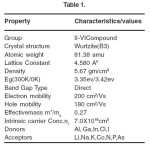 |
Table 1 Click here to View table |
Electrical and magnetic properties
The electrical properties of RE-doped ZnO films with different thicknesses were investigated by Hall effect measurements as shown in figure1, using the van der Pauw geometry as shown in figure 2. For Hall measurements in vander Pauw geometry]17-18], four Au contacts are evaporated, of which the I(V) characteristics exhibits an ohmic behaviour and have resistances ranging from 100 Ω to 1 kΩ determined by Hall measurement in which magneto transport measurements are performed in two point geometry with a magnetic field H perpendicular to the sample plane as shown in figure 1. They depend on the film composition, oxygen partial pressure, and substrate temperature during the growth process.
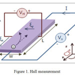 |
Figure 1. Hall measurement Click here to View figure |
Our investigations revealed that the free electron concentration, n, is independent of temperature over the investigated range 20–320 K. Measurements for films with different thicknesses revealed that for films grown on Al2O3 substrates the carrier concentration is decreasing with increasing film thickness, contrary to our expectations. This behaviour was observed in ZnO films grown on Al2O3 substrates and is explained by the presence of a thin, degenerate, highly conducting interface layer between substrate and film.The results for films grown on SiO2 show that the carrier concentration is increasing with increasing film thickness (Fig.3). This allows us to assume that most carriers in the highly conducting interface layer for the films grown on Al2O3 are produced by Al diffusion from the substrate. RBS has a sensitivity for Al as low as 3%, not allowing the investigation of Al depth profile in our films.
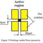 |
Figure 2.Working vander Pauw geometry Click here to View figure |
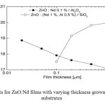 |
Figure 3. Hall results for ZnO:Nd films with varying thickness grown on Al2O3 or SiO2 substrates Click here to View figure |
The magnetic behavior of the films was investigated by magnetotransport measurements at different temperatures. We investigated the MR behaviour in different magnetic fields. Negative MR ratio was detected in ZnO:RE films. In Fig. 4 we present results obtained at 5 K for ZnO films doped with different Nd contents or Al. A much pronounced negative MR is detected in ZnO:RE as compared to ZnO:Al, meaning that the signal from the ZnO:RE films is given by the RE incorporated into the ZnO lattice. The carrier concentration in the ZnO:Al film is 2 × 1020 cm−3 while for the ZnO:RE films is in the range 1 × 10¹⁷ to 1 × 1019 cm−3. With increasing temperature, MR approaches zero very quickly. No anomalous Hall effect was detected, even at low temperatures. The negative MR can be interpreted as a paramagnetic response of the RE ions to the applied magnetic field [6], meaning the RE ions do not interact via exchange mechanisms. This statement is also supported by the lack of anomalous Hall effect. We should remark that the films presented in Fig. 4 have thicknesses around 20 nm, meaning only degenerate layers. For thicker films attention must be paid, because the path of the current through the film cannot be easily established, the results being difficult to interpret. It could happen that current passes only through the thin degenerate layer near the film–substrate interface.
Other methods are used to investigate the local magnetic properties on film surface. Magnetic force microscopy (MFM), for example, is used to detect the presence of magnetic domains on the film surface. As an example, this technique revealed bubble like magnetic domains withdiameters around 4 μm on a ZnO:RE film containing 0.1 at.% Nd, grown at 639 _C and 0.012 Torr on a-plane Al2O3 (Fig. 5). Such domains are characteristic for films with uniaxial magnetic anisotropy, the easy axis being perpendicular to film surface. The homogenous distribution of magnetic domains in Fig. 5 indicates that the signal is not due to clusters eventually formed during the growth process.
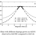 |
Figure 4. MR for ZnO films with different dopings grown on Al2O3. A much higher ratio is observed in ZnO:RE compared to ZnO:Al. Click here to View figure |
 |
Figure 5. Bubble-like magnetic domains on a ZnO film doped with 0.1 at% Nd Click here to View figure |
Conclusions
We prepared and investigated ZnO films doped with different contents of Nd. The films were grown on a-plane Al2O3 or SiO2 substrates. Hall investigations of electrical properties revealed the presence of a degenerate, highly conducting, film–substrate interface layer for the films grown on Al2O3; such an effect can be avoided, for example, by using SiO2 substrates.Magnetotransport measurements indicated no anomalous Hall effect, but a pronounced negative magnetoresistance ratio that can be interpreted as a paramagnetic response of the system to the applied magnetic field. We would like to proceed with the surface sensitive techniques for investigating magnetic properties of ZnO:RE thin films.
Future Work
This section recommends additional experiments and characterization techniques that would extend the information obtained in the present study. Thin film samples with dopant concentrations slightly higher and lower than 3 atomic % should be fabricated in parallel with investigation of post annealing effects on observed paramagnetism. The effects of oxygen partial pressure during deposition should also be studied. Another very useful study would be to attempt to deposit very smooth and very thin films by varying the deposition rate and substrate temperature while also studying growth on conductive substrates. This would allow for characterization of magnetic field dependent electrical properties.
Acknowledgement-We are very thankful to Dr. Nidhi Sharma Lecturer HPES for her guidance and support.
References
- S.J. Pearton, D.P. Norton, K. Ip, Y.W. Heo, T. Steiner, J. Vac. Sci. Technol. B 22 (2004) .
- T. Dietl, H. Ohno, F. Matsukura, J. Cibert, D. Ferrand, Science 287 PP 1019 (2010)
- K. Sato, H. Katayama-Yoshida, Jpn. J. Appl. Phys Part 2 Lett. 39, L555 (2000).
- J. Newey, “Spintronics holds promise for more efficient devices,” Compound Semiconductor, vol.10, pp. 23, (2011).
- S. A. Chambers and Y. K. Yoo, “New materials for spintronics,” MRS Bulletin, vol. 28, pp. 706, (2009).
- M. Diaconu, H. Schmidt, H. Hochmuth, M. Lorenz, G. Benndorf, J. Lenzner, D. Spemann, A. Setzer, K.W. Nielsen, P. Esquinazi, M. Grundmann, Thin Solid Films 486.117(2005).
- P. Sharma, A. Gupta, K.V. Rao, F.J. Owens, R. Sharma, R. Ahuja, J.M. Osorio Guillen, B. Johansson, G.A. Gehring, Nat. Mater. 2, 673 (2003).
- K. Ueda, H. Tabata, T. Kawai, Appl. Phys. Lett. 79,988 (2001).
- S. Dhar, O. Brandt, M. Ramsteiner, V.F. Sapega, K.H. Ploog, Phys. Rev. Lett. 96, (2005).
- Jagadisch Chennupati and Stephen J. Pearton, editors. Zinc oxide: bulk, thin films and nanostructures. Elsevier, (2006).
- Klaus Ellmer and Andreas Klein, editors. Transparent conductive zinx oxide. Springer, (2008).
- A. Mofor, Physica Status Solidi C 3, 1104 (2006).
- Wikipedia: Pulsed laser deposition — wikipedia, the free encyclopedia (2008).URLhttp://en.wikipedia.org/w/index.php?title=Pulsed_laser_deposition&oldid=259950687.
- D. Chrisey (editors): Pulsed laser deposition of thin films. Wiley,New York (1994).
- Y. Zheng , Journal of Crystal Growth 274(1-2), 156 (2011).
- J.L. Zhao, Journal of Crystal Growth 276, 507 (2008).
- H. Tampo, A. Yamada, P. Fons, H. Shibata, K. Matsubara, K. Iwata, S. Niki, K. Nakahara, H. Takasu, Appl. Phys.Lett. 84,4412 (2004) .
- M. Csontos, T. Wojtowicz, X. Liu, M. Dobrowolska, B. Janko, J.K. Furdyna, G. Mihaly, Phys. Rev. Lett. 95,227203.

This work is licensed under a Creative Commons Attribution 4.0 International License.
![]()
A New Edition of Web of Science
Journal Impact Factor
2022: 0.5
Five Year: 0.8
Journal is Indexed in

Cabells Whitelist
![]()


